📌 Product Overview
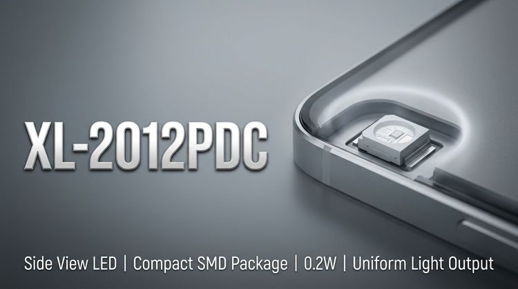
💡 The XL-2012PDC is an NPN silicon phototransistor packaged in a standard 0805 (2012 metric) SMD footprint, measuring 2.0x1.25x0.8mm.
📌 Primary Function: Designed to convert infrared light signals into electrical current, with peak sensitivity at 880nm, making it ideal for discrete optical sensing circuits.
👇 Design Focus: The component utilizes a black epoxy colloid to filter visible light noise, enhancing signal stability in ambient light conditions.
🔌 Typical Applications
- Consumer Electronics: Infrared receivers for remote control systems.
- Industrial Automation: Photoelectric switches and object detection counters.
- Smart Systems: Encoder wheels for intelligent cars and robotics.
- Instrumentation: Optical isolation and pulse detection in smart meters.
- Security: Camera monitoring heads for light intensity activation.
⚙️ Key Technical Specifications
| Parameter | Symbol | Test Conditions | Min | Typ | Max | Unit |
|---|---|---|---|---|---|---|
| Collector-Emitter Breakdown Voltage | BVCEO | IC=100μA | 85 | — | — | V |
| Peak Sensitivity Wavelength | λp | — | — | 880 | — | nm |
| Photocurrent (λp=850nm) | ICE | Ee=1mW/cm², VCE=5V | 300 | 400 | — | μA |
| Current Amplification Factor | hFE | VCE=5V, IC=2mA | 200 | — | 300 | — |
| Collector Dark Current | ICEO | VCE=20V | — | — | 30 | nA |
| Spectral Bandwidth | λ0.5 | — | 700 | — | 1100 | nm |
💡 Note: Photocurrent grading is available (e.g., Rank C6: 0.3–0.6mA) for tighter signal control in precision designs.
🚨 Absolute Maximum Ratings & Process Limits
| Parameter | Symbol | Rating | Unit | Notes |
|---|---|---|---|---|
| Collector-Emitter Voltage | VCEO | 30 | V | Do not exceed to prevent breakdown. |
| Emitter-Collector Voltage | VECO | 5 | V | Reverse bias limit. |
| Operating Temperature | Topr | -40 ~ +85 | °C | Standard industrial range. |
| Storage Temperature | Tstg | -40 ~ +85 | °C | MSL Level 3 (Floor life 168 hours). |
| Soldering (Reflow) | Tsol | 260 | °C | Max 6 seconds (Infrared process). |
| Soldering (Manual) | Tsol | 300 | °C | Max 3 seconds; Iron power < 30W. |
| Antistatic Ability | ESD | 2000 | V | Human Body Model (HBM). |
🔒 Reliability: Qualified for high-humidity storage (85°C / 90-95% RH) and thermal cycling (-40°C to +105°C).
📦 Package, Dimensions & Assembly Notes
- Package Type: 0805 (EIA Standard).
- Dimensions: 2.0mm (L) x 1.25mm (W) x 0.8mm (H).
- Tape & Reel: Compliant with EIA standards for automated SMT placement.
- Soldering Profile:
- Lead-Free: Peak temp 255°C (Max 5-10s above 217°C).
- Leaded: Peak temp 235°C (Max 10-15s above 183°C).
- Cleaning: Isopropyl alcohol recommended (≤50°C for 30s). Ultrasonic power should not exceed 300W.
📈 Assembly Tip: Minimize mechanical stress on the component during heating to avoid micro-cracks in the epoxy.
🛒 Sourcing & Supply Considerations
- BOM Optimization: Verify the photocurrent rank code to match circuit sensitivity requirements.
- Supply Chain: Confirm MSL 3 packaging integrity if the manufacturing environment exceeds standard humidity.
- Cross-Reference: Check footprint compatibility with standard 0805 land patterns to reduce stencil design costs.
- Quality Control: Request ESD test data if the application involves high static environments (e.g., robotic joints).
❓ Frequently Asked Questions
Q: What is the recommended land pattern for the XL-2012PDC?
A: The datasheet suggests a standard footprint compatible with EIA 0805 specifications. A pad design slightly larger than the component terminals (approx. 1.2mm x 0.9mm per terminal) is recommended to ensure sufficient solder fillet strength during reflow.
Q: Can this phototransistor be used for outdoor applications?
A: While the operating temperature supports -40°C to +85°C, the device is primarily designed for indoor infrared communication. For outdoor use, additional optical filtering and potting may be required to protect against UV degradation and moisture ingress.
Q: How do I interpret the photocurrent grading?
A: The component is binned based on photocurrent output (e.g., Code C6 = 0.3-0.6mA). Selecting a specific bin allows designers to limit the gain variance of the sensor circuit, ensuring consistent response times across mass-produced units.
Q: What are the constraints for manual rework?
A: Manual soldering is permitted for repair only. Use a soldering iron ≤30W with a tip temperature below 300°C. Contact time must be limited to 3 seconds per pin, and only one soldering attempt is recommended to prevent thermal damage to the internal die.
Q: Is the XL-2012PDC compatible with lead-free soldering processes?
A: Yes, the component is rated for lead-free (Pb-Free) infrared reflow soldering with a peak temperature of 255°C. However, it should not undergo more than two reflow cycles to maintain reliability.
Q: How should I store components if the packaging is opened?
A: The XL-2012PDC has a Moisture Sensitivity Level (MSL) of 3. If the vacuum-sealed bag is opened, the components should be mounted within 168 hours (1 week) or baked according to IPC/JEDEC J-STD-033 standards to prevent popcorning during reflow.