💡 Key Takeaways
• HBF offers 16x HBM capacity with comparable bandwidth at claimed lower cost
• NAND's 1-2 order of magnitude latency gap versus DRAM limits HBF's standalone viability
• Industry players diverge: SK Hynix pursues HBF, Samsung/AMD push HBM4 and CXL alternatives
🎯 Opening
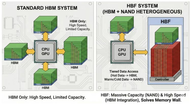
SK Hynix and SanDisk's proposed High Bandwidth Flash (HBF) aims to address AI memory capacity constraints by stacking NAND flash with HBM-level bandwidth using TSV technology. The concept promises 3TB capacity at 8TB/s bandwidth—16x HBM3e capacity at one-fifth estimated cost.
📊 What's Changing
HBF architecture combines NAND flash stacks with silicon-through-vias (TSV) to achieve HBM-level bandwidth while offering massive capacity expansion. The proposed H³ hybrid approach separates read-only data (model weights, precomputed KV cache) stored in HBF from dynamic KV cache in HBM, with 40MB SRAM buffer (LHB) mitigating NAND's 20µs access latency.
🔍 Why Old Assumptions No Longer Work
The H³ paper's performance claims rely on critical assumptions: read-only workloads where model weights and shared precomputed KV cache remain unchanged throughout inference; deterministic, sequential access patterns enabling accurate prediction and pre-fetching; 40MB SRAM buffer achieving sufficient hit rates (implicitly 80%+) to hide most HBF latency.
📗 Data / Comparison
Simulation results show impressive gains: 1.25x throughput at 1M tokens, 6.14x at 10M tokens, and 2.69x performance-per-watt. Even halving HBF bandwidth maintains advantage. But these results require all assumptions to hold simultaneously.
⚡ Implications for OEM / EMS / Procurement
NAND's physical limitations present fundamental barriers. DRAM cells read/write capacitor charge via transistor switching in 10-20ns. NAND cells move electrons via tunneling effect requiring high voltage and longer time—25-100µs. This represents a 1,000x difference. 40MB SRAM can mitigate but not solve this gap. Once SRAM misses, the difference fully exposes.
🚀 How Smart Teams Are Responding
HBM4 from Samsung/SK Hynix/Micron targets mass production 2026 with 50% bandwidth increase (1.5TB/s per cube). Samsung's HBM-PIM executes simple operations within memory. CXL 3.0 offers memory pooling via PCIe 6.0 at 256GB/s for TB-scale expansion. Software optimizations like FlashAttention-3 and FlashDecoding++ reduce bandwidth requirements without hardware investment.
✨ Closing
HBF represents an innovative approach to AI memory constraints but faces fundamental physics and market adoption challenges. The industry pursues multiple technical pathways—HBM evolution, CXL expansion, and software optimization—to solve capacity expansion differently. OEMs evaluating HBF adoption should validate against actual production workloads, considering total cost of ownership beyond NAND's attractive per-GB pricing.