📌 Product Overview
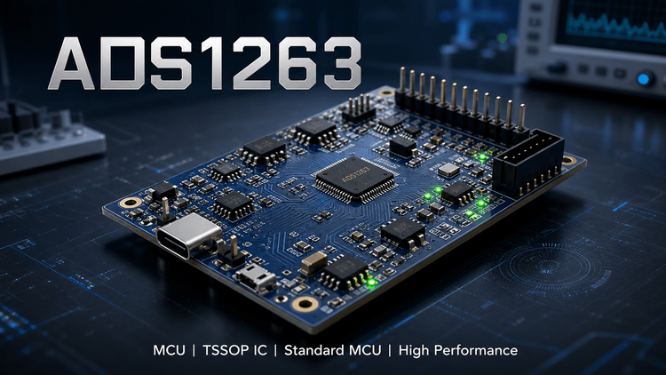
The ADS1263 is a high-precision, 32-bit Delta-Sigma ADC designed for industrial sensor measurement. 💡 Unlike standard microcontrollers (MCUs) or logic ICs, this device integrates a primary 32-bit ADC and a secondary 24-bit ADC, specifically targeting weigh scales, strain gauges, and thermocouples. The core value for engineering teams lies in its ultra-low noise (7nV-RMS) and integrated PGA, which eliminate the need for external signal conditioning components in high-accuracy factory automation and process control systems.
🎯 Typical Applications & Design Context
This component is optimized for sensor front-ends requiring high resolution and industrial noise immunity.
- Weigh Scales & Load Cells: The 32-bit resolution and low gain drift (0.5 ppm/°C) ensure stability in precision weighing, critical for OEMs in industrial automation.
- Temperature Measurement: Integrated excitation current sources allow direct connection to RTDs (e.g., PT100), simplifying BOM layout for temperature controllers.
- Process Analytics: The auxiliary 24-bit ADC enables continuous background system monitoring (e.g., supply voltage or temperature) without interrupting the primary sensor measurement, a key requirement for safety-critical instrumentation.
📊 Key Technical Specifications
Ref: Datasheet SBAS661C (Rev May 2021)
| Parameter | Value/Condition | Engineering Impact |
|---|---|---|
| Resolution | 32-bit (Primary) / 24-bit (Aux) | Enables detection of micro-changes in sensor resistance; vital for high-precision load cells. |
| Data Rate | 2.5 SPS to 38,400 SPS | Supports fast sampling (38.4 kSPS) for quick settling or slow (2.5 SPS) for maximum noise rejection. |
| Input Noise | 7 nV RMS (at 2.5 SPS, Gain=32) | 🚀 Critical Parameter: Determines the floor of measurable weight; lower noise allows for smaller scale resolution without drifting. |
| PGA Gain | 1 to 32 | Flexible scaling of small sensor signals (e.g., thermocouples) without external op-amps. |
| Offset Drift | 1 nV/°C | Guarantees measurement stability across the industrial temperature range (-40°C to +125°C). |
⚠️ Absolute Maximum Ratings & Process Limits
Exceeding these limits risks permanent damage to the input PGA or reference circuitry.
| Parameter | Rating | 🔥 Failure Mode / Validation Note |
|---|---|---|
| Analog Input Voltage | AVDD + 0.3V to AVSS - 0.3V | Exceeding this (e.g., surge from sensor) can cause latch-up or breakdown of the CMOS input PGA. |
| Operating Temp | -40°C to +125°C | Mass production validation must ensure the internal 2.5V reference drift (2 ppm/°C) is accounted for in high-temp environments. |
| Reflow Temp | 260°C (Max) | Standard TSSOP profile; however, moisture sensitivity (MSL) must be adhered to prevent popcorn cracking of the 28-pin package. |
🧩 Package, Dimensions & Assembly Notes
- Package Type: TSSOP (28-pin)
- Body Size: 9.70 mm × 4.40 mm
- Pitch: Standard 0.65 mm pitch.
- SMT Validation: As a Precision ADC, the PCB layout is as critical as the component. The exposed thermal pad (if present on variant) or ground pins must be connected to a quiet analog ground plane. During SMT, ensure the 2.5V internal reference settling time is observed after power-up; incorrect decoupling (see Section 11.1 of datasheet) will result in conversion noise failures.
🔍 Procurement & Sourcing Insights
- Lead Time & Availability: As a specialized TI precision analog component, the ADS1263 typically carries longer lead times (12-20 weeks) compared to standard logic. Procurement must forecast accurately.
- Risk Warning: This is not a generic commodity. Cross-sourcing is difficult due to the unique register map and dual-ADC architecture.
- Authenticity: High-value precision ADCs are frequent targets for cloning. Fake chips often have higher noise floors or fail high-temperature drift tests.
- LDeepAI Recommendation: Verify traceability codes. For alternative validation, the ADS1262 (Pin-to-Pin compatible, but lacks the 24-bit auxiliary ADC) is the only safe drop-in replacement if the secondary channel is unused in firmware.
❓ FAQ
Q: Can I replace the ADS1263 with the ADS1262 without modifying the PCB?
A: Yes. The ADS1262 and ADS1263 are pin-to-pin compatible. However, the ADS1262 lacks the auxiliary 24-bit ADC. If your firmware relies on the second ADC for background diagnostics, switching to the '1262 will result in a functional failure unless the code is rewritten to ignore the missing channel.
Q: What is the most common failure mode during mass production validation?
A: Noise injection from digital lines. Because this is a 32-bit ADC (sensitive to nV levels), routing digital SPI/UART lines too close to analog inputs (AIN0-AIN9) often causes failure to pass "Noise Performance" specs. Ensure proper separation of Analog and Digital grounds.
Q: How do I verify if a supplied batch is genuine?
A: Authentic TI chips have specific laser-etched markings on the TSSOP package. Functional testing should focus on the Offset Drift (1 nV/°C). Clones often fail here, showing significant drift when the board temperature changes from 25°C to 85°C.
Q: Is the internal 2.5V reference sufficient for 0.1% accuracy scales?
A: Yes, but with a caveat. The internal reference has a drift of 2 ppm/°C. For high-precision industrial scales exposed to wide temperature swings, an external low-drift reference might be required to maintain system-level accuracy over the full -40°C to +125°C range.