🧭 Key Takeaways
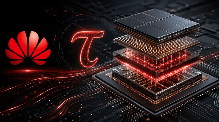
• The Event: Huawei presented the Tau (τ) Scaling Law at IEEE ISCAS 2026 in Shanghai, positioning it as a post-Moore framework for semiconductor and system evolution.
• The Cause: As transistor shrinkage faces physical, economic, and geopolitical limits, Huawei is prioritizing signal delay, interconnect efficiency, and system-level data movement over pure node migration.
• The Implication: 3D packaging, chiplet integration, and high-density interconnects become critical execution layers, but Tau Scaling is broader than packaging alone.
🔍 Huawei’s Tau Scaling Law: From Geometry Scaling to Time Scaling
Huawei’s Tau Scaling Law, also referred to in Chinese media as “韬(τ)定律,” proposes a shift in semiconductor optimization from geometric scaling to time scaling. Instead of asking how much smaller a transistor can become, the framework asks how quickly signals, instructions, and data can move across devices, circuits, chips, and systems.
Huawei introduced the concept on May 25, 2026, at the IEEE International Symposium on Circuits and Systems in Shanghai. According to Huawei, the law targets the reduction of the time constant τ across multiple levels: device, circuit, chip, and system. The company links this approach to technologies such as LogicFolding, software-architecture-chip co-design, and its Lingqu interconnect bus.
For OEM, EMS, and engineering teams, the key point is that Tau Scaling is not simply another packaging roadmap. It is a system-performance framework. Packaging is one of the most visible execution layers, but the real objective is shorter data paths, lower RC delay, higher compute density, and better workload-level efficiency.
⚙️ Why Huawei Is Emphasizing Tau Scaling Now
The timing is important. Huawei has been restricted from accessing advanced semiconductor manufacturing tools and leading-edge foundry capacity since U.S. export controls intensified after 2019. Reuters reported that Huawei is using Tau Scaling and LogicFolding as part of a strategy to improve performance without depending solely on frontier lithography.
Huawei claims that it has already designed and mass-produced 381 chips over six years based on Tau Scaling-related practices. The company also says a Kirin chip expected in autumn 2026 will adopt LogicFolding, and that high-end chips based on the framework could reach transistor density equivalent to 1.4 nm-class processes by 2031. These are company claims and still require broader third-party validation under production conditions.
The market reaction has been mixed. Industry coverage recognizes the strategic importance of reducing data-movement latency, but analysts have also flagged familiar advanced-packaging risks: heat dissipation, yield, design-tool maturity, and verification complexity.
📦 How Tau Scaling Relates to 3D Packaging
3D packaging and Tau Scaling are closely related, but they are not the same concept.
3D packaging is a manufacturing and integration method. It stacks or places multiple dies closer together through technologies such as hybrid bonding, through-silicon vias, silicon interposers, fan-out packaging, or high-density redistribution layers. Its goal is to increase bandwidth, reduce interconnect distance, improve energy efficiency, and integrate heterogeneous functions.
Tau Scaling is an optimization principle. It defines time delay, not transistor size alone, as the central metric. Under this logic, 3D packaging becomes valuable because it can shorten physical data paths and reduce the energy cost of communication between logic, memory, analog, and I/O functions.
This relationship is similar to the role of TSMC’s 3DFabric platform, which combines 3D silicon stacking and advanced packaging technologies such as SoIC, CoWoS, and InFO to support high compute density, energy efficiency, low latency, and heterogeneous integration.
In other words, 3D packaging is one of the strongest physical tools for achieving Tau Scaling goals, but Tau Scaling also extends into circuit layout, architecture, software scheduling, memory hierarchy, and system interconnect.
Comparison Table: 3D Packaging vs. Tau Scaling
| Dimension | 3D Packaging | Tau Scaling |
|---|---|---|
| Core definition | A manufacturing and integration method for placing multiple dies or chiplets closer together | A system optimization principle centered on reducing time delay |
| Primary focus | Physical proximity, interconnect density, bandwidth, and heterogeneous integration | End-to-end latency, data movement efficiency, architectural delay, and system response time |
| Typical technologies | Hybrid bonding, TSV, silicon interposer, fan-out, RDL, CoWoS, SoIC, InFO | Architecture optimization, memory hierarchy design, circuit placement, software scheduling, interconnect planning |
| Main engineering goal | Reduce physical distance between functional blocks | Reduce the time required to complete useful computation |
| Key value | Enables high-bandwidth, low-energy die-to-die communication | Provides a performance framework beyond transistor scaling alone |
| Relationship to Moore’s Law | Extends system capability when monolithic scaling becomes harder | Reframes scaling around latency and usable system performance |
| Role in AI / HPC systems | Connects logic chiplets, HBM, cache, and I/O in dense packages | Measures whether the full compute system can move and process data fast enough |
| Limitation | Packaging alone cannot solve architecture, memory, or software bottlenecks | Requires physical implementation methods such as 3D packaging to deliver practical gains |
| Strategic implication | One of the strongest physical tools for latency and bandwidth improvement | A broader design philosophy that can guide chip, package, board, and software decisions |
🧩 LogicFolding: Packaging, Layout, or Architecture?
Huawei’s LogicFolding is the technical bridge between Tau Scaling and 3D integration. Public descriptions suggest that it breaks the boundary of traditional two-dimensional circuit layout by reorganizing logic to shorten critical paths and reduce resistance-capacitance loading.
This makes LogicFolding more nuanced than conventional package stacking. It appears closer to a hybrid concept across circuit architecture, physical design, and 3D integration. If implemented successfully, it could improve effective density without requiring the same lithographic node as leading-edge foundries.
However, the challenge is that shorter interconnects do not automatically translate into reliable system gains. Vertical integration can create thermal concentration, mechanical stress, test-access constraints, and yield loss. These issues become more difficult when logic, memory, and analog functions are integrated at tighter pitches.
For procurement and engineering teams, the practical question is not whether the term “Tau Scaling” replaces Moore’s Law. The more useful question is whether suppliers can demonstrate stable yield, validated thermal design, repeatable assembly, and predictable lifecycle support.
🧠 Why This Matters for AI Hardware and High-Performance Systems
AI accelerators are increasingly limited by memory bandwidth, data movement, and package-level integration rather than raw transistor count alone. This is why 2.5D and 3D packaging have become central to high-end GPU, FPGA, network switch, AI training, and data-center hardware roadmaps. ASE, for example, describes 2.5D/3D IC packaging as important for HBM integration in high-end GPUs, FPGAs, AI accelerators, and data-center networking.
Huawei’s Tau Scaling aligns with this broader industry direction. The framework says that system value comes from reducing the time and energy cost of data movement. This is exactly why chiplet architectures, HBM integration, CoWoS-class interposers, SoIC-class 3D stacking, and advanced substrates have become strategic bottlenecks.
Yole Group estimates that the advanced packaging market could reach $83 billion by 2030, reflecting strong demand from AI, HPC, and heterogeneous integration platforms.
🔒 Supply Chain Implications for OEM and EMS Teams
For OEM and EMS procurement teams, the Huawei Tau Scaling discussion should be read as a signal of where semiconductor competition is moving.
First, packaging capability is becoming a strategic capacity item. Advanced nodes remain important, but package-level integration, substrate availability, thermal material selection, and test coverage now directly affect system performance and delivery risk.
Second, supplier qualification needs to move earlier in the design cycle. When performance depends on die-to-die links, vertical stacking, HBM proximity, and package warpage control, late-stage sourcing decisions create higher redesign risk.
Third, the bill of materials will shift from component cost toward integration cost. Substrates, interposers, thermal interface materials, high-density PCBs, and validation services may become more constrained than standard IC supply.
Fourth, engineering teams should evaluate “density-equivalent” claims carefully. A chip may claim 1.4 nm-class density equivalence, but OEMs still need application-level data: power under sustained workload, junction temperature, memory bandwidth, software stack maturity, and long-term reliability.
📈 Strategic View: Tau Scaling Does Not Replace 3D Packaging; It Increases Its Importance
The most accurate way to interpret Huawei’s Tau Scaling Law is not as a rejection of existing semiconductor roadmaps, but as a reframing of what matters after geometric scaling slows.
Moore’s Law focused on placing more transistors into the same area. 3D packaging focuses on placing functional blocks closer together. Tau Scaling focuses on reducing the time penalty of computation and communication across the full stack.
That makes 3D packaging more important, not less. If the industry optimizes for latency, bandwidth density, and energy per bit, then package architecture becomes a core part of silicon performance rather than a downstream assembly step.
For global OEMs, EMS providers, and hardware architects, the practical takeaway is clear: future platform competitiveness will depend not only on which process node a chip uses, but also on how effectively logic, memory, interconnect, substrate, package, cooling, and software are co-designed.
✅ Conclusion
Huawei’s Tau Scaling Law is best understood as a system-level response to the slowdown of traditional scaling and the constraints of advanced manufacturing access. Its relationship with 3D packaging is direct but not identical: 3D packaging provides the physical proximity needed to reduce delay, while Tau Scaling provides the broader optimization target.
The concept still faces execution risks in thermal management, yield, design tools, and third-party performance validation. But its direction is consistent with the wider semiconductor industry: future performance gains will come from shorter paths, denser integration, and tighter co-design between silicon and systems.