📌 Product Overview
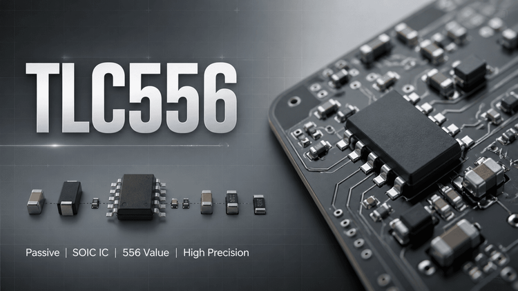
The TLC556 from Texas Instruments is a dual CMOS monolithic timing circuit — functionally the CMOS counterpart of the bipolar NE556, with an identical 14-pin footprint. Each half contains two comparators, a flip-flop, and a discharge transistor, supporting astable and monostable operation up to 2MHz.
Because it is built in CMOS rather than bipolar process, it delivers 2mW typical power at 5V, rail-to-rail output swing, and operation from a 2V–15V single supply. The critical selection variables are the CMOS-level trigger/threshold behavior, output source current (10mA vs 100mA sink), and temperature grade (C: 0–70°C, I: −40–85°C, M: −55–125°C).
🎯 Typical Applications & Design Context
- Precision timing and time-delay generation — high input impedance supports smaller timing capacitors, improving delay accuracy vs NE556
- Pulse generation, PWM, and PPM — rail-to-rail CMOS output drives logic directly without level-shifting
- Sequential timing and linear ramp generators — CONT pin allows shifting the 1/3–2/3 VDD thresholds
- Battery-powered equipment — low static current and reduced supply spikes during output transitions minimize decoupling capacitor count vs bipolar 556 designs
💡 If your PCB was designed around NE556, the TLC556 typically drops in — but validate the output drive direction (weak source, strong sink) before reusing circuits that source current into loads.
📊 Key Technical Specifications
| Parameter | Value | Design Impact |
|---|---|---|
| Supply voltage | 2V – 15V | Single-supply, wide-window logic design |
| Trigger level | ≈ 1/3 VDD | Same topology as NE556 |
| Threshold level | ≈ 2/3 VDD | Adjustable via CONT pin |
| Output sink current | 100mA typical | Drives LEDs, small relays directly |
| Output source current | 10mA typical | ⚠️ Weak source — buffer high-side loads |
| Max frequency | 2MHz | Astable/monostable timing ceiling |
| Power consumption | 2mW typ @ 5V | Battery-friendly |
| Output logic | CMOS / TTL / MOS compatible | Rail-to-rail swing |
⚠️ Absolute Maximum Ratings & Process Limits
⚠️ Key boundaries from the datasheet that govern production survival:
| Limit | Boundary | Failure Mode if Exceeded |
|---|---|---|
| Supply voltage (max) | 15V operating window | Latch-up or junction damage if 24V lines back-feed the timer rail |
| Input voltage (TRIG/THRES/CONT/RESET) | Not to exceed VDD | Inputs driven above VDD during power sequencing damage comparators |
| Unused inputs | Must tie to defined logic level | Floating TRIG/RESET causes false triggering in noisy SMT lines |
| Temperature grade C / I / M | 0–70°C / −40–85°C / −55–125°C | Using C-grade in industrial enclosures causes timing drift and field returns |
💡 E-E-A-T field note: The most common mass-production failure with this family is not electrical overstress — it's uncommitted TRIG or RESET pins left floating on cost-reduced PCB revisions, producing intermittent output glitching that appears only on certain production lots. Enforce pulldowns on all unused control pins in DFM review.
🧩 Package, Dimensions & Assembly Notes
| Package | Ordering Suffix | Pins | Notes |
|---|---|---|---|
| SOIC (D) | TLC556C/I D | 14 | Standard SMT reflow; verify MSL per reel label |
| PDIP (N) | TLC556C/I/M N | 14 | Wave solder / hand-fit; common in legacy industrial boards |
| LCCC (FK) / CDIP (J) | TLC556M only | 20 / 14 | Military grade; special handling and sockets |
- Pinout: D/J/N share the same pin map; the FK LCCC-20 uses a different pin arrangement with NC pins — do not footprint-share
- Both timer halves are independent; RESET is active-low and overrides all inputs
- Tie CONT with a 0.01–0.1µF bypass capacitor for noise immunity in switching-noise-heavy layouts
🔍 Procurement & Sourcing Insights
- 🔒 Counterfeit exposure is high: TLC556 is a 40-year-old legacy part frequently re-marked in gray-market channels. Verify date codes, lot traceability, and packaging integrity — LDeepAI validates source channel and provides tested, traceable stock.
- 📈 Suffix matters: TLC556C vs TLC556I vs TLC556M are different orderable parts at different price points; industrial customers ordering C-grade to save cost create field-failure liability.
- 🚀 Alternatives: NE556 (bipolar) is pin-compatible but not power/performance-identical; TI's TLC555 (single) and other CMOS 556 equivalents exist — request validation data before drop-in substitution.
- Samples and low MOQ available — contact LDeepAI for lead time confirmation on I and M grades.
❓ FAQ
Q: Can TLC556 directly replace NE556 on an existing PCB?
A: Pin-compatible and functionally interchangeable. However, NE556 sources significantly more output current and requires larger decoupling capacitors. Most designs work, but validate output source-current loading and supply-spike behavior.
Q: Why is my timing period different from the NE556 design calculation?
A: CMOS high input impedance allows — and often requires — smaller timing capacitors. Reuse of large electrolytic timing caps with high leakage causes period error; switch to film or low-leakage types.
Q: What is the difference between TLC556C, I, and M?
A: Temperature rating only: C = 0–70°C, I = −40–85°C, M = −55–125°C (also in FK/J ceramic packages). Suffix must match the orderable part number.
Q: Can the output drive a relay directly?
A: Sinking 100mA is typical — low-side relay coils with a flyback diode are feasible. Sourcing is only 10mA; high-side drive needs a buffer transistor.
Q: How do I avoid false triggering in production?
A: Tie all unused inputs (especially RESET and TRIG) to defined logic levels, bypass CONT, and keep trigger pulse widths within datasheet limits.