📌 Product Overview
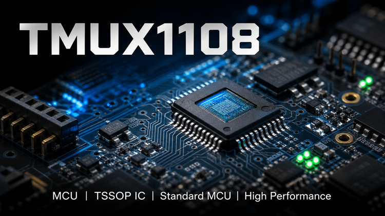
The Texas Instruments TMUX1108 is a precision CMOS 8:1 single-ended multiplexer designed for high-accuracy measurement systems. Operating across a wide 1.08V to 5.5V supply, it features ultra-low leakage current (3pA) and low charge injection (1pC). For engineering teams, the critical selection variables are signal integrity and fail-safe logic; for procurement, it involves navigating package availability (PW vs. RSV) and long-term delivery stability for industrial-grade applications.
🎯 Typical Applications & Design Context
👇 The TMUX1108 excels in high-impedance, precision-sensing environments where signal integrity is non-negotiable:
- Medical Equipment (Ultrasound, Patient Monitoring): The 3pA low leakage and 1pC charge injection prevent analog signal distortion from high-impedance sensors.
- Industrial Automation (PLC, ATE): Wide operating temperature (-40°C to +125°C) and fail-safe logic ensure robust performance against aggressive power sequencing.
- Battery Monitoring Systems: 8nA low supply current minimizes power draw in portable or continuous-monitoring circuits.
📊 Key Technical Specifications
| Parameter | Specification | Engineering & Procurement Impact |
|---|---|---|
| Configuration | 8:1, 1-Channel | Allows routing of 8 sensors to a single precision ADC. |
| Supply Voltage (VDD) | 1.08V to 5.5V | 🔒 High compatibility with modern low-voltage MCUs. |
| On-Resistance (Ron) | 2.5Ω | Minimizes voltage drop across the switch. |
| Leakage Current | 3pA | Prevents ADC measurement errors in high-impedance circuits. |
| Charge Injection | 1pC | Reduces transient voltage glitches during channel switching. |
| Logic Compatibility | 1.8V TTL/CMOS | Enables direct interface with low-voltage processors. |
⚠️ Absolute Maximum Ratings & Process Limits
| Rating | Limit | Failure Risk & E-E-A-T Insight |
|---|---|---|
| Operating Temperature | -40°C to +125°C | Exceeding this derates Ron significantly, leading to measurement drift. |
| ESD Protection (HBM) | 2000V | Standard handling limits; requires strict ESD controls during SMT. |
| Supply Voltage (VDD) | Connected to GND to specific max | 💡 Fail-safe logic prevents damage if control pins are biased before VDD is fully ramped up. |
🚨 Mass Production Reality: In actual SMT or end-use, exceeding thermal limits during reflow can degrade the 3pA leakage integrity. The fail-safe logic is a critical defensive parameter—if sequencing is ignored during PCB power-up, latch-up can occur, destroying the IC and potentially the upstream ADC.
🧩 Package, Dimensions & Assembly Notes
The TMUX1108 is available in two distinct package options, dictating different PCB design and sourcing strategies:
- PW Package (TSSOP, 16-pin): 5.0mm × 6.4mm. Preferred for standard automated optical inspection (AOI) yield and manual debugging. Standard moisture sensitivity level (MSL 1) supports flexible floor life.
- RSV Package (UQFN, 16-pin): 2.6mm × 1.8mm. ✨ Ideal for space-constrained portable devices. However, procurement must verify EMS capabilities for ultra-small pitch paste printing and reflow profiles to avoid tombstoning.
🔍 Procurement & Sourcing Insights
- Alternative Validation: When evaluating cross-brand drop-in replacements (e.g., from ADI or Nexperia), verify the charge injection (1pC) and 3pA leakage specs, as competitors often mask poor high-temperature leakage performance.
- Package Lead Times: The RSV (UQFN) package faces significantly higher allocation constraints compared to the legacy TSSOP. Plan forecasts accordingly.
- Channel Authenticity: Counterfeit MUX ICs often exhibit degraded on-resistance (Ron) or leaked charge injection. LDeepAI recommends strictly verifying date codes and utilizing decap testing for unfranchised channel sourcing to ensure traceability.
❓ FAQ
Q: Can I hot-swap or apply signals to the TMUX1108 before powering up VDD?
A: Yes. This device features Fail-Safe Logic, meaning the logic control pins (A0, A1, A2, EN) can tolerate voltages up to 5.5V before VDD is applied, preventing device damage or latch-up during power sequencing.
Q: What is the primary cross-brand alternative risk when replacing the TMUX1108?
A: The primary risk is signal degradation. While generic 8:1 MUX parts may have identical pinouts, they often have higher charge injection and off-state leakage at 125°C, which will ruin high-impedance sensor measurements in medical or ATE equipment.
Q: How does the 1.8V logic compatibility affect PCB design?
A: It allows direct connection to modern 1.8V MCUs without level-shifting circuitry, reducing BOM cost and board area.
Q: Are the PW (TSSOP) and RSV (UQFN) packages pin-to-pin compatible?
A: No, they have entirely different physical footprints and pin assignments (see datasheet Figure 5-1 vs 5-2). PCB redesign and SMT stencil modifications are mandatory if switching packages to resolve allocation shortages.