📌 1. Product Overview
The Texas Instruments ADS1263 is a high-precision, 32-bit Delta-Sigma (ΔΣ) Analog-to-Digital Converter (ADC) designed for industrial sensor measurement. Unlike standard SAR ADCs, it integrates a Programmable Gain Amplifier (PGA), a precision 2.5V internal voltage reference, and a unique auxiliary 24-bit ADC for continuous background monitoring (e.g., temperature compensation while measuring strain).
Targeting high-end applications like weigh scales, thermocouples, and RTD sensors, the ADS1263 resolves micro-volt signals with exceptionally low noise (7nV-RMS). For the engineering team, this device shifts the complexity from analog circuit design to digital filter configuration and PCB layout discipline. It is not merely a component; it is a complete analog front-end (AFE) system-on-chip.
📌 2. Typical Applications & Design Context
The ADS1263 is specifically architected for applications where signal stability outweighs speed. While it supports up to 38.4 kSPS, its strength lies in low-frequency, high-resolution measurement.
- 🎯 Weigh Scales & Strain Gauges: The high PGA gain (up to 128) allows direct connection to bridge sensors without external amplification. The 50/60Hz rejection is critical here to eliminate mains noise in industrial environments.
- 🌡️ Temperature Measurement (RTD/Thermocouples): The integrated sensor excitation current sources simplify PCB routing, but require careful calibration to avoid self-heating errors in the sensor itself.
- ⚡ Process Automation: The auxiliary ADC allows for simultaneous system diagnostics (monitoring supply voltage or a second sensor) without interrupting the primary measurement loop.
📌 3. Key Technical Specifications
| Parameter | Value/Condition | Design Impact |
|---|---|---|
| Resolution | 32-bit (Effective) | Enables detection of minute signal changes; requires extremely low-noise reference design. |
| Integrated PGA | Gains 1 to 128 | Eliminates need for external op-amps, reducing component count and board space. |
| Offset Drift | 1 nV/°C | Critical Parameter: Ensures calibration validity across industrial temperature ranges (-40°C to +125°C). |
| Noise (RMS) | 7 nV (at 2.5 SPS, Gain=32) | Defines the noise floor; limits the smallest detectable physical change in the sensor. |
| Auxiliary ADC | 24-bit | Allows for background system monitoring (e.g., cold-junction compensation) without CPU intervention. |
| Internal Reference | 2.5 V (Drift 2 ppm/°C) | Acceptable for many applications, but external low-drift references (e.g., REF50xx) may be needed for top-tier accuracy. |
💡 Engineering Insight: While "32-bit" captures attention, the 7nV noise and 1nV/°C drift are the actual specifications that determine if your design succeeds in a noisy factory environment.
📌 4. Absolute Maximum Ratings & Process Limits
Exceeding these parameters risks immediate silicon damage or latent lifetime failure (parametric drift).
| Parameter | Rating | 🔥 E-E-A-T Validation Note (Failure Mode) |
|---|---|---|
| AVDD to AGND | -0.3V to +6.0V | Latch-up Risk: Exceeding 6V, even transiently during hot-plug, can trigger CMOS latch-up, destroying the device. |
| Analog Input Voltage | -0.3V to (AVDD + 0.3V) | ESD Diode Conduction: If input protection fails (e.g., surge on sensor cable), current flows through ESD structures. Must add external TVS/schottky clamps for field-wired sensors. |
| Junction Temp (Tj) | 150°C | Thermal Runaway: Poor PCB thermal design (no copper pours under the TSSOP pad) can cause self-heating, degrading the internal 2.5V reference accuracy. |
| Reflow Soldering | 260°C (Peak) | Package Warpage: TSSOP-28 packages can warp if thermal profiles are too aggressive, leading to open joints on the center ground pins (exposed pad). |
⚠ Critical Process Warning: The "Effective 32-bit" performance relies on the Absolute Maximum Ratings never being approached. Design your protection circuitry assuming the sensor input cable is cut and shorted to 24V industrial power.
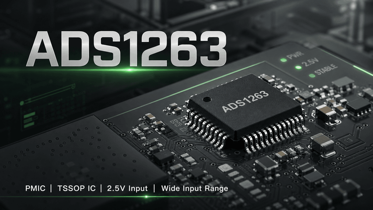
📌 5. Package, Dimensions & Assembly Notes
- Package:28-pin TSSOP (Thin Shrink Small Outline Package).
- Dimensions: 9.70 mm × 4.40 mm.
- Land Pattern: The thermal pad (if present, or the central ground pins) must be soldered to the PCB ground plane to dissipate power from the internal PGA.
✨ SMT Validation Guide:
- Stencil Design: Due to the fine pitch (0.65mm typical), ensure stencil aperture reduction for thermal pads to prevent solder wicking and voiding.
- Moisture Sensitivity: This device is moisture-sensitive. If the dry pack is broken, baking is required (per IPC/JEDEC J-STD-033) to prevent "popcorning" (delamination) during reflow.
- Layout Criticality: Do not route digital signals (SPI SCLK) under the analog input pins. The TSSOP form factor is small; grounding the exposed pad is the only heat dissipation path.
📌 6. Procurement & Sourcing Insights
From a supply chain perspective, the ADS1263 is a high-mix, low-volume (HMLV) component compared to general-purpose MCUs.
- 💰 Cost vs. Availability: The ADS1263 is often "Not Recommended for New Designs" (NRND) or strictly controlled by TI distribution. Long lead times (20+ weeks) are common.
- 🚨 Alternative Validation: Do not assume drop-in compatibility. While the ADS1262 is pin-compatible (lacking the auxiliary ADC), moving to competitors like Analog Devices (AD7175) or Cirrus Logic requires a complete PCB spin and software driver rewrite due to register map differences.
- 🔒 Authenticity: Given the high value and low volume, the ADS1263 is a target for ghost shift/counterfeit parts in open markets.
- LDeepAI Protocol: We strictly source from authorized franchised distributors or employ advanced X-Ray/Decap authentication for secondary market buys.
👉 Decision for Procurement: Secure stock early for the pilot run. If lead times exceed project timelines, budget for a redesign using an alternative, or engage a broker with verified traceability (CoC) only.
📌 7. FAQ
Q1: Can I replace the ADS1263 with the cheaper ADS1262 without changing the PCB?
A: Yes, electrically they are pin-to-pin compatible. The ADS1262 lacks the auxiliary 24-bit ADC (pins may be NC). If your firmware uses the second ADC for temperature compensation, you must update your software or redesign the sensor compensation algorithm.
Q2: The datasheet mentions "Single-cycle settled" conversions. What does this mean for my MCU timing?
A: It means the ADC data is valid immediately after the DRDY (Data Ready) pin goes low, unlike older ΔΣ ADCs requiring multiple settling cycles. This allows faster channel switching (scanning), but your MCU must be fast enough to fetch the data before the next cycle starts.
Q3: Is the internal 2.5V reference good enough for a Class III weigh scale?
A: Likely not. For legal-for-trade applications requiring <10ppm total drift, the internal reference (2 ppm/°C) consumes too much of the error budget. You should use an external reference like the REF5025 or LM4140.
Q4: What is the biggest risk in mass production using the TSSOP-28 package?
A: Tombstoning or solder joint defects on the fine-pitch leads if the PCB footprint is not optimized. Additionally, moisture sensitivity means you must strictly follow the floor-life (exposure) limits before reflow to prevent internal cracking.