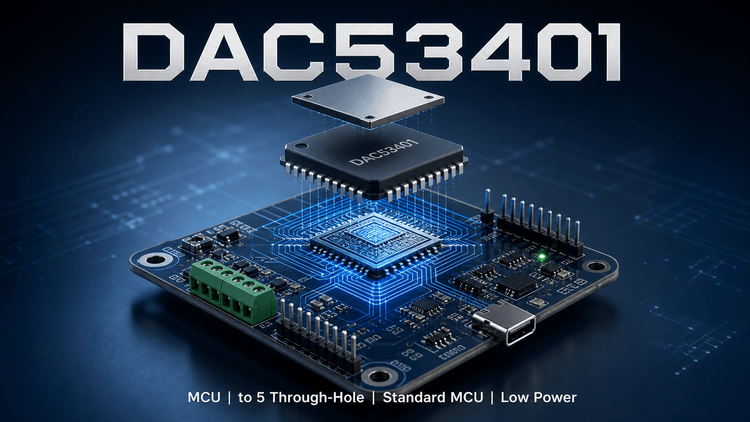
📌 Product Overview
The DAC53401 is a 10-bit, voltage-output Digital-to-Analog Converter (DAC) integrating a nonvolatile memory (NVM) and a PMBus™ compatible I²C interface. Designed by Texas Instruments in a tiny 2mm × 2mm WSON package, this device is engineered for space-constrained industrial and automotive applications. It functions as a programmable voltage reference or waveform generator, capable of operating from 1.8V to 5.5V. For design engineers, the critical selection variables are its integrated EEPROM (which reduces MCU overhead at startup) and its flexible power-up behavior, making it ideal for closed-loop power supply margining and sensor bias systems.
🎯 Typical Applications & Design Context
- Rack Servers & Power Supplies: The integrated PMBus interface and feedback (FB) pin enable direct connection to DC/DC controllers for voltage margining and output voltage trimming without discrete DAC resistors.
- Automotive USB Charging & Lighting: With an operating temperature up to +125°C and AEC-Q100 potential (implied by automotive apps), it suits in-cabin USB port controllers and emergency lighting drivers.
- Factory Automation (PLC): The programmable waveform generation (square, ramp, sawtooth) allows this tiny IC to replace complex amplifier circuits for generating test signals or alarm tones in industrial control panels.
- Why it fits: The combination of NVM and internal reference eliminates the need for an external LDO or EEPROM in BOM-constrained designs.
📊 Key Technical Specifications
| Parameter | Value/Condition | Design Impact |
|---|---|---|
| Resolution | 10-bit (DAC53401) | Provides 1024 steps; ~1mV resolution at 2V full scale. |
| Supply Voltage | 1.8 V to 5.5 V | Wide range allows direct connection to 3.3V logic or 5V industrial rails. |
| Interface | I²C (PMBus compatible) | Supports Standard/Fast/Fast+ modes; logic high threshold (VIH) ensures noise immunity. |
| Output Drive | Buffered Voltage Output | Can drive low-impedance loads directly; however, check capacitive load stability (≤ 100pF recommended). |
| Nonvolatile Memory | Internal EEPROM | Stores register settings (waverforms, gain) for instant recall on power-up. |
| Package | 8-pin WSON (2mm × 2mm) | Ultra-small footprint requires precise thermal pad soldering. |
⚠️ Absolute Maximum Ratings & Process Limits
| Parameter | Rating | 💡 E-E-A-T Engineering Reality Check |
|---|---|---|
| VDD Supply Voltage | –0.3V to 6.0V | Exceeding 6V, even briefly during hot-plug events (e.g., USB debugging), can rupture the input ESD structures. Design Tip: Add a TVS diode if the supply line is exposed to external transients. |
| Input Current (Any Pin) | ±50 mA | Latch-up Risk: If the analog output (OUT) is forced to a voltage higher than VDD (e.g., power rail sequencing error), current can latch the IC. Ensure VDD ramps up before external bias voltages or design the load to be passive. |
| Total Power Dissipation | Dependent on PCB layout | In the 2x2mm WSON package, the thermal pad is the only heat path. Poor soldering of the thermal pad (via voids in SMT) will cause the internal junction to overheat even at low electrical loads, leading to thermal shutdown or drift. |
| ESD Rating | HBM 2kV, CDM 500V | Handling bare dies during PCB rework requires strict grounding; otherwise, the high-impedance input pins are vulnerable to CDM events from plastic fixtures. |
🧩 Package, Dimensions & Assembly Notes
The WSON-8 (2mm × 2mm) package features a thermal pad on the bottom (Pin 9 equivalent).
- SMT Validation: The CAP pin requires an external capacitor (0.5µF to 15µF) for the internal LDO. Critical Validation Point: If this capacitor is missing or placed too far from the pin (>10mm trace), the internal LDO may oscillate, causing noise on the DAC output.
- Stencil Design: Ensure adequate aperture ratio for the center thermal pad to avoid solder voiding. A void rate >30% significantly degrades thermal performance.
- Moisture Sensitivity: WSON packages are typically moisture-sensitive. Baking is required if the dry pack is exposed to the floor for more than the specified floor life (usually 72 hours) before reflow to prevent popcorning delamination.
🔍 Procurement & Sourcing Insights
- Alternative Risks: While pin-compatible with the 8-bit DAC43401, swapping to the 10-bit DAC53401 requires I²C register map updates (resolution changes).
- Supply Chain: The 2x2mm WSON package is a high-volume standard for TI, but lead times can extend to 20+ weeks during semiconductor shortages.
- Counterfeit Alert: In the open market, re-marked 8-bit versions are sometimes sold as 10-bit. LDeepAI recommends sourcing only through TI-authorized channels or using X-Ray inspection to verify the die markings and bond wire structure for mass production.
- Design Validation: Request samples for Hot Soldering tests to ensure the thermal pad wets correctly on your specific PCB surface finish (ENIG vs. OSP).
❓ FAQ
Q: Can I use the DAC53401 to generate a PWM signal for motor control?
A: It is not a PWM generator. It generates voltage waveforms (ramps/squares). For motor PWM, you would feed this DAC's output into the reference pin of a separate PWM comparator or controller.
Q: What happens if I leave the CAP pin floating?
A: The internal LDO will likely become unstable. This results in high-frequency noise appearing on your analog output, rendering the ADC readings useless. You must connect the specified capacitor.
Q: Is the PMBus interface backwards compatible with standard I²C?
A: Yes. The device supports standard (100kHz), fast (400kHz), and fast+ (1MHz) modes. You can control it via a standard MCU I²C peripheral without needing a dedicated PMBus master, though the protocol commands utilize PMBus formats.
Q: How does the feedback (FB) pin work in practice?
A: The FB pin allows the DAC to "adjust" its output based on an external voltage. It is primarily used for power supply margining (e.g., slightly raising/lowering a server rail to test CPU stability). For general DAC use, FB is typically connected to AGND or used for gain scaling.