📌 Product Overview
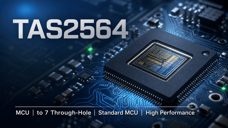
The TAS2564 is a high-performance digital input Class-D smart amplifier featuring an integrated 13-V Class-H boost converter. Designed primarily for mobile phones, tablets, and portable Bluetooth speakers, it delivers up to 7 W of peak power into an 8 Ω load. For design engineers, the critical selection variables are its 256-level boost tracking (optimizing battery life) and integrated I/V sense (protecting speakers in small form factors). This device moves beyond simple amplification by acting as a system-level power management node for battery-operated audio.
🎯 Typical Applications & Design Context
Based on its high efficiency and integrated boost architecture, the TAS2564 is ideally suited for space-constrained, battery-powered devices requiring high audio output:
- Smartphones & Tablets: 📱 Utilizes the I2S/TDM interface for direct connection to application processors, leveraging the 13 V boost to drive micro-speakers without external amplifiers.
- Portable Bluetooth Speakers: 🔊 Maximizes playtime through the 256-level algorithmically controlled boost, which reduces average power consumption while maintaining peak headroom.
- Consumer Audio Docks: Benefits from the low EMI spread spectrum operation to minimize interference with nearby wireless radios (Wi-Fi/BT).
📊 Key Technical Specifications
| Parameter | Value | Condition/Note |
|---|---|---|
| Output Power | 7 W | 0.1% THD+N, 8 Ω @ 3.8V |
| Efficiency | 83.5 % | 1 W Output Power |
| Supply Voltage (VBAT) | 2.7 V to 5.5 V | Battery operating range |
| Integrated Boost | 13 V Class-H, 256-level | Algorithmically controlled |
| Interface | I2S/TDM (8 ch, 32-bit) | Up to 96 KSPS |
| SNR | 110 dB | @ 1% THD+N |
| Idle Channel Noise | 10 µVrms (Receiver mode) | Excellent noise floor |
⚠️ Absolute Maximum Ratings & Process Limits
| Parameter | Rating | E-E-A-T Critical Comment |
|---|---|---|
| VBAT Input Voltage | -0.3 V to 6.0 V | Exceeding 6.0V risks immediate gate oxide destruction of the internal boost FETs. |
| Total Power Dissipation | Limited by Tj (150°C) | In compact layouts, insufficient thermal vias under the DSBGA will trigger thermal shutdown during high-bass passages. |
| ESD Rating (HBM) | ±2000 V | Handling requires standard ESD precautions; the DSBGA pins are sensitive to static discharge during pick-and-place. |
| Operating Temp | -40 °C to 85 °C | 🌡️ Derating power is mandatory in high-ambient environments (e.g., automotive dash mounts) to prevent "Brown-Out" resets. |
🧩 Package, Dimensions & Assembly Notes
- Package Type: 36-Pin DSBGA (2.63 mm × 2.46 mm).
- Pitch: The array requires precise X-Ray inspection during SMT validation.
- Thermal Strategy: The DSBGA dissipates heat primarily through the PCB ground plane. Mandatory: Use at least 4-6 thermal vias under the thermal pads (BGND/PGND) connected to a large copper pour area.
- Layout Sensitivity: Keep the inductor (L1) and boost capacitors (C1/C2) as close as possible to the pins to minimize radiated EMI.
🔍 Procurement & Sourcing Insights
- Availability: As a specialized audio IC, the TAS2564 often has longer lead times than generic codecs. Do not substitute with standard Class-D amps without revising the boost inductor footprint.
- Supply Chain: Beware of "Ghost Shift" components in the Huaqiangbei market; marked parts may fail I2C communication due to internal firmware mismatches.
- Validation: 💡 Secure engineering samples early to validate the PurePath Console GUI configuration files; transferring register settings (I/V coefficients) to a new alternative lot is a high-risk failure point.
❓ FAQ
Q: Can I use a fixed 5V supply instead of a battery on VBAT?
A: Yes, the specs allow 2.7V–5.5V. However, the "Battery Tracking" peak voltage limiter algorithm will behave differently; you must re-tune the registers via I2C to prevent premature clipping at fixed voltage.
Q: Is this a drop-in replacement for the TAS2563?
A: No. While the package (DSBGA 2.63x2.46) may look similar, the internal boost converter architecture and register maps differ significantly. Direct swapping will likely result in no sound or distorted output due to incorrect boost voltage ramping.
Q: What is the biggest risk during SMT assembly?
A: Solder bridging on the DSBGA pitch. Due to the dense pin grid (A1-F6), insufficient solder paste volume or misalignment can short the VDD (1.8V) and VBAT (5V) lines, causing device failure upon power-up.
Q: Why do I need the I/V Sense feature?
A: For Speaker Protection. It monitors real-time current and voltage to keep the transducer within its Safe Operating Area (SOA), preventing burnout in compact sealed enclosures where heat dissipation is poor.