📌 Product Overview
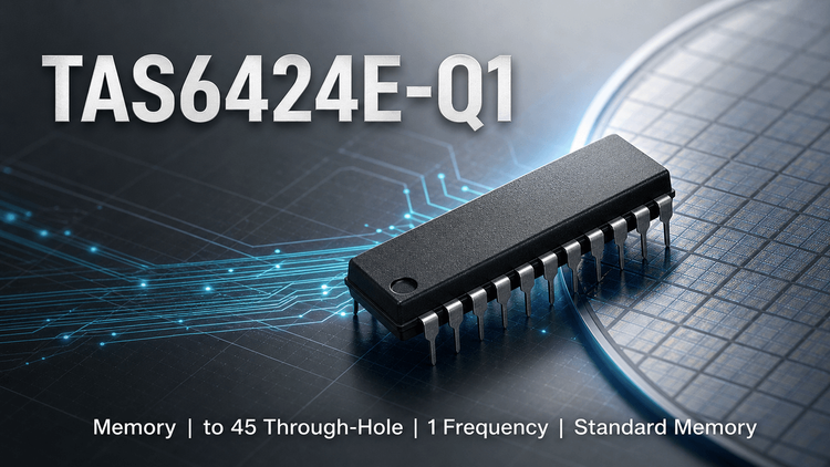
The TAS6424E-Q1 is a high-performance, digital-input Class-D audio amplifier designed by Texas Instruments specifically for automotive infotainment systems. It is optimized to drive 4 Ω or 2 Φ loads in automotive head units and external amplifiers, delivering up to 45 W per channel into 2 Ω. For global OEMs and EMS providers, the critical selection factors for this component are its AEC-Q100 Grade 1 qualification (operating from –40°C to +125°C) and its integrated 40 V load-dump protection, which simplifies system-level power supply design. Unlike generic amplifiers, the TAS6424E-Q1 integrates advanced load diagnostics and I2C control, allowing engineers to detect misconnected speakers or tweeter impedance without requiring complex external circuitry.
🎯 Typical Applications & Design Context
This device is specifically engineered for the automotive supply chain, addressing the stringent environmental and acoustic requirements of modern vehicles. It is best suited for:
- Automotive Head Units: 🚗 As the central playback engine, where PCB space is limited, and the 2.1 MHz switching frequency allows for smaller inductors and filters.
- External Amplifier Modules: 📈 Utilizing the PBTL (Parallel Bridge-Tied Load) mode to drive subwoofers with up to 150 W of power.
- e-Cockpit Systems: ✨ Where high-resolution audio (up to 32-bit/96 kHz) is required for premium user experiences.
The device suits these scenarios because its integrated DC diagnostics run without input clocks, enabling faster manufacturing test times, while the CISPR25 Class-L5 compliance reduces the need for heavy EMI shielding cans in the final assembly.
📊 Key Technical Specifications
| Parameter | Specification | Notes for Engineering/Procurement |
|---|---|---|
| Output Power | 45 W (2 Ω) / 27 W (4 Ω) @ 14.4 V, 10% THD | Sufficient for premium automotive audio tiers. |
| Switching Freq | 2.1 MHz (AM Band) | Enables cost-optimized ferrite bead filters; reduces PCB area. |
| Input Interface | I2S or TDM (16-32 bit) | Supports high-res audio; compatible with modern SoC outputs. |
| Load Diagnostics | DC/AC Diagnostics | Detects open/short loads and tweeter impedance (up to 6 kΩ). |
| Supply Voltage | 4.5 V to 26.4 V | Wide input range supports start/stop events and battery sag. |
| Efficiency | Class-D Operation | Reduces need for large heatsinks compared to Class-AB. |
⚠️ Absolute Maximum Ratings & Process Limits
Adhering to these ratings is non-negotiable for high-volume automotive success.
| Rating | Value | E-E-A-T Practical Insight |
|---|---|---|
| Supply Voltage | 40 V (Load Dump) | While tolerant, sustained operation near 40V degrades junction life; ensure clamping. |
| Operating Temp | –40°C to +125°C (TA) | ⚠️ Derating is required in enclosed head units without active airflow. |
| Input Voltage | –0.3 V to 7.0 V | Exceeding 7V on digital pins can latch the I2C interface, requiring board rework. |
| Power Dissipation | Dependent on PCB ΘJA | Poor thermal pad soldering (voiding >20%) will trigger thermal shutdown at <50% rated power. |
E-E-A-T Comment: The most common failure mode in mass production is thermal shutdown caused by insufficient thermal relief around the Thermal Pad (PAD). If the center pad is not properly soldered to the internal ground layers, the device cannot dissipate heat, leading to intermittent audio cutting (clipping) even at low volumes.
🧩 Package, Dimensions & Assembly Notes
- Package Type: HSSOP-56 (Heat Slug / PowerPAD).
- Dimensions: 18.41 mm × 7.49 mm.
- Assembly Criticality: The center pad acts as the primary thermal path.
- 👇 Stencil Design: Ensure aperture ratio allows 50%-80% solder paste coverage on the thermal pad to avoid tombstoning or floating.
- 🔒 SMT Profile: Compatible with standard automotive reflow profiles (peak temp 245°C max). However, moisture sensitivity is a concern; if floor life is exceeded, the device may suffer "popcorning" under the slug.
- ⚡ Layout: Keep the high-frequency switching loops (PVDD to PGND) as small as possible to prevent radiated emissions failing CISPR25.
🔍 Procurement & Sourcing Insights
From a supply chain perspective, the TAS6424E-Q1 presents specific risks that must be managed:
- Supply Volatility: As a specialized automotive IC, lead times can extend beyond 52 weeks during industry shortages.
- Alternative Validation: ⚠️ Do not assume pin-compatibility with the non-automotive version. Verify if your stock is "TI Genuine" or "Cypress" marked. Counterfeit devices often fail the "DC Diagnostics" self-test during bootup.
- MOQ & Samples: Typically sourced in Tape & Reel (4000+ units). For prototyping, ensure samples are date-coded <12 months to avoid oxidation on the thermal pads.
- Risk Control: LDeepAI recommends cross-referencing the date code against TI's shipping markings database to prevent gray-market stock infiltration.
❓ FAQ
Q: Can I replace the TAS6424E-Q1 with the TAS6424-Q1 directly?
A: Generally no for new designs requiring the latest features. While pin-compatible, the 'E' variant supports a higher current limit (7.2 A vs 6.5 A) and non-latching clip detect features. Substituting with a lower current part may result in thermal shutdown during high-bass audio transients.
Q: What is the biggest risk in SMT assembly?
A:Solder joint voiding. The exposed thermal pad must have proper via-in-pad design. If x-ray inspection shows voiding over 30%, the thermal resistance will skyrocket, causing the chip to trigger over-temperature protection prematurely.
Q: Why does my design fail CISPR25 EMI tests?
A: The 2.1 MHz switching frequency helps, but layout is king. Ensure the differential output traces are tightly coupled and kept away from the AM antenna input. Using non-optimized output inductors (DCR too high) can also create ringing that radiates EMI.
Q: How do I verify authenticity in the open market?
A: Verify the package laser markings. Authentic TI parts have a distinct, crisp laser-etched lot code and date code. Perform a simple I2C read-back of the Device ID register (0x00) on the bench; counterfeit clones often return 0xFF or garbage data.