📌 Product Overview
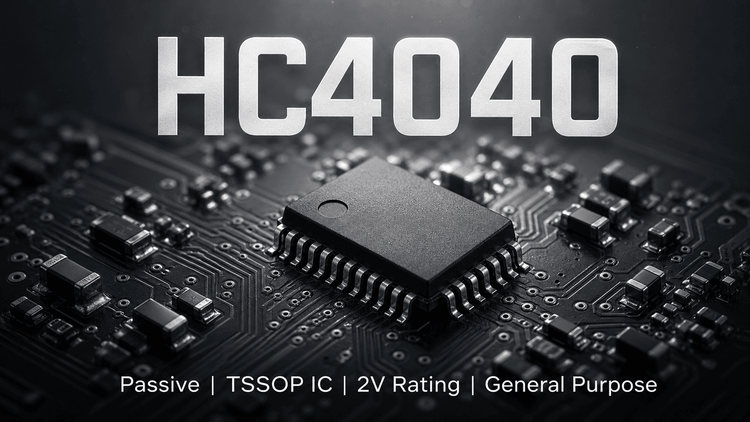
The SN74HC4040 is a 12-stage asynchronous binary counter designed for high-speed logic applications. Unlike synchronous counters, this device ripple-clocks through 12 stages, making it ideal for frequency division and long-duration timing without complex firmware. It is manufactured by Texas Instruments under the "HC" (High-speed CMOS) family, balancing speed and power consumption.
For procurement and engineering teams, the critical selection variables are the wide voltage range (2 V to 6 V), which offers flexibility in both 3.3 V and 5 V systems, and the asynchronous clear (CLR) function, which is vital for system reset reliability. Understanding the propagation delay accumulation is essential for high-frequency clock designs.
🎯 Typical Applications & Design Context
This component is frequently utilized in digital subsystems where event counting or frequency scaling is required.
- Frequency Division: Efficiently divides high-frequency clock signals down to lower frequencies for timer interrupts or clock gating.
- Time-Delay Circuits: Utilizes the ripple-clock effect to create long delays, leveraging the 12-stage count depth (up to 4096 counts).
- Industrial Controls: Often found in legacy interface logic or power management sequencing due to its robust 5 V tolerance and noise immunity.
The HC family's ability to drive up to 10 LSTTL loads makes it suitable for buffering clock signals across PCB planes without immediate need for additional driver circuitry.
📊 Key Technical Specifications
| Parameter | Condition/Min | Nom/Typ | Max | Unit |
|---|---|---|---|---|
| Supply Voltage (VCC) | 2 | 5 | 6 | V |
| Input Logic High (VIH) | @ 4.5V VCC | - | 3.15 | V |
| Input Logic Low (VIL) | @ 4.5V VCC | 1.35 | - | V |
| Clock Freq (Max) | @ 6V VCC | - | 12 | MHz (Typ) |
| Power Dissipation (CC) | - | 80 | - | µA |
| Output Drive Current | @ 5V VCC | - | ±4 | mA |
| Operating Temp | SN74 Series | -40 | +85 | °C |
💡 Design Insight: While the device supports a 6 V supply, the propagation delay ($t_{pd}$) typically varies by ~12 ns. Ensure your timing budget accounts for the cumulative delay of all 12 stages if using the final output (Q11) as a sync signal.
⚠️ Absolute Maximum Ratings & Process Limits
Exceeding these parameters invites immediate failure or latent reliability defects.
| Stress Parameter | Rating | Unit | Failure Mode / E-E-A-T Note |
|---|---|---|---|
| Supply Voltage | -0.5 to 7 | V | ⚡ Latch-up Risk: Exceeding 7V (even transiently) can trigger parasitic thyristor structures, causing catastrophic short circuits. |
| Input Clamp Current | ±20 | mA | 🔥 Bond Wire Damage: ESD events exceeding this current limit will vaporize bond wires before the protection diodes can recover. |
| Continuous Output Current | ±25 | mA | 📉 Thermal Runaway: Driving LEDs or heavy loads near this limit without derating will degrade the metallization, increasing resistance over time. |
| Storage Temperature | -65 to 150 | °C | 🧊 Moisture Ingress: For TSSOP/SOIC packages, extended exposure outside MSL limits post-seal break causes "popcorning" during reflow. |
👇 Validation Rule: Always verify the Input Transition Rise/Fall Time. The datasheet specifies a maximum rise/fall time (e.g., 500ns @ 4.5V). Slow-rising signals (common in sensor interfaces) can cause oscillation or double-clocking of the intermediate stages, leading to unpredictable count totals.
🧩 Package, Dimensions & Assembly Notes
Physical compatibility is the primary hurdle for cross-branding.
- Footprint Verification: The SN74HC4040D (SOIC-16) is the standard industry footprint. However, the PW (TSSOP-16) package has a nominal body size of 5.00 mm × 4.40 mm. Tighter pitch (0.65mm) on TSSOP requires laser-drilled stencils for proper paste release.
- Thermal Management: The Junction-to-Ambient ($\theta_{JA}$) resistance for the SOIC (D) package is 73°C/W. In a 70°C ambient environment with minimal air flow, the junction temperature will approach thermal limits quickly if self-heating occurs.
- MSL Level: Typically MSL 3 (168 hours) for moisture sensitivity. Bake components if the floor life is exceeded to prevent internal cracking during SMT reflow.
🔍 Procurement & Sourcing Insights
Sourcing logic ICs requires navigating a market flooded with "functional clones" that fail under thermal stress.
- Supply Chain Risk: The SN74HC4040 is a mature, multi-source part (on/offshore). However, subtle differences in input hysteresis exist between TI and secondary competitors.
- Authenticity: Scrutinize lead finish and laser markings. Counterfeit HC series often have inconsistent laser etching depth or "grainy" plastic molding compound surfaces.
- Alternative Evaluation: When validating a non-TI alternative, strictly test the Clock (CLK) to Output (Q) propagation delay at both 2.0V (worst-case speed) and 4.5V. A generic part may fail at lower voltages where speed drops significantly.
- Availability: TI guarantees 12-year lifecycle support. For new designs, avoid the SN54 (Military) series unless cost-insensitivity allows for the extended temperature range.
❓ FAQ
Q: Can I replace SN74HC4040 with a CD4040 directly?
A: Generally, NO for mixed-voltage systems. While pin-compatible, the CD4000 series is much slower and requires higher voltage (often >5V) to reach similar speeds. The HC4040 is designed for 2V-6V operation with TTL drive capability, whereas the CD4040 may not reliably sink/source current required by TTL loads at 3.3V.
Q: What happens if the Clear (CLR) pin is left floating?
A: A floating CLR pin acts as an antenna, susceptible to EMI. This can cause unintended resets (random counter resets to zero). TI design guidelines mandate tying unused inputs to VCC or GND. For CLR, tie to GND (via a resistor if isolation is needed) or a logic-controlled line.
Q: Why does my count seem to skip values at high frequency?
A: This is likely Ripple Delay accumulation. The HC4040 is asynchronous; the clock must ripple through all 12 previous stages to increment the last bit. At high frequencies (near 12MHz), the total propagation delay may exceed the clock period, causing the MSB to miss the clock edge. Use a synchronous counter for high-speed systems.
Q: How do I identify the package type from the label?
A: Check the suffix.
- D: SOIC (Wide body, surface mount standard).
- N: PDIP (Through-hole, for prototyping).
- PW: TSSOP (Thin, for high-density layouts).
Verify the PCB footprint matches these suffixes before volume procurement to avoid line stoppages.