📌 Product Overview
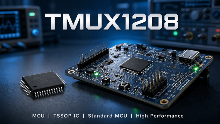
The TMUX1208 is a general-purpose 5-V bidirectional 8:1, 1-channel CMOS multiplexer utilizing a single-ended architecture. Manufactured by Texas Instruments, it is designed for routing analog and digital signals to MCU ADCs. Engineers must prioritize its 1.08V to 5.5V operating supply, 5Ω on-resistance, and 1.8V logic compatibility during system selection and PCB layout.
🎯 Typical Applications & Design Context
💡 Target environments include HVAC systems, smoke detectors, video surveillance, and battery-powered portable electronics.
👇 Why it fits: The ultra-low 10nA supply current extends battery life in always-on sensor monitors. Furthermore, the "Fail-Safe Logic" feature allows control pins to be biased before VDD is fully ramped up, which is critical for hot-plug scenarios or sequenced power domains in complex industrial systems.
📊 Key Technical Specifications
| Parameter | Specification | Engineering Implication |
|---|---|---|
| Configuration | 8:1, 1-Channel | Routes 8 sensor inputs to 1 MCU ADC port. |
| Operating Voltage (VDD) | 1.08V to 5.5V | Wide rail-to-rail support for modern low-voltage MCUs. |
| On-Resistance (Ron) | 5 Ω (typical) | Minimizes signal attenuation for analog sensors. |
| Transition Time | 14 ns | Fast switching suitable for high-speed data acquisition. |
| Logic Compatibility | 1.8 V Logic | Direct interfacing with modern low-voltage processors without level shifters. |
| Special Feature | Fail-Safe Logic, Break-Before-Make | Prevents shorting between multiplexed channels during state transitions. |
⚠️ Absolute Maximum Ratings & Process Limits
🚀 Exceeding these boundaries guarantees permanent silicon damage or latent field failures.
| Limit Parameter | Absolute Max |
|---|---|
| Voltage (VDD to GND) | -0.5V to 7.0V |
| I/O Voltage (Sx, D) | -0.5V to VDD+0.5V |
| ESD Protection (HBM) | 2000V |
| Operating Temperature | -40°C to +125°C |
🔒 E-E-A-T Validation Insight: The most common mass-production failure for this device is violating the I/O voltage limit. If an external sensor signal is applied to the source pins (Sx) while the system VDD is floating or at 0V, the internal ESD protection diodes will forward-bias, creating a parasitic power rail. This causes unpredictable system resets or catastrophic latch-up. Always ensure signal trace power sequencing respects the I/O absolute maximum.
🧩 Package, Dimensions & Assembly Notes
The TMUX1208 is available in standard 16-pin TSSOP (5.00mm × 4.40mm) and compact 16-pin QFN (2.60mm × 1.80mm) packages.
- SMT Assembly: The QFN package requires precise stencil aperture design to avoid solder bridging on the 0.5mm pitch.
- Thermal Management: The QFN features a center thermal pad; ensure adequate vias to the ground plane.
- Layout: Place a 0.1µF decoupling capacitor as close to the VDD pin as possible to absorb switching noise.
🔍 Procurement & Sourcing Insights
📈 As a high-volume TI component, the TMUX1208 frequently faces allocation constraints and extended lead times.
- Alternative Validation: The TMUX1209 is a pin-for-pin drop-in alternative if a 4:1 dual-channel architecture is acceptable for your routing. Standard cross-references like CD4051B exist, but verify timing differences.
- Channel Risk: This component is heavily targeted by counterfeiters in the open market due to its wide application in security cameras.
- Traceability: Always demand original factory DC (Date Code) documentation and bonded-source verification.
❓ FAQ
Q: What is the core selection difference between TMUX1208 and TMUX1209?
A: The TMUX1208 is a single-channel 8:1 multiplexer. The TMUX1209 is a dual-channel 4:1 (or differential 4:1) multiplexer. Ensure your MCU ADC scanning logic matches the channel architecture before freezing the BOM.
Q: Do I need an external level shifter for the address pins?
A: Not necessarily. The device features 1.8V logic compatible thresholds, meaning a standard 1.8V GPIO from an MCU can successfully drive the A0, A1, A2, and EN pins even when VDD is operating at 5V.
Q: What is the most critical design rule to prevent field failure?
A: Never apply voltage to the analog/digital signal pins (Sx or D) before powering up the VDD pin. Violating this power sequencing causes current injection through the internal ESD diodes, leading to latch-up. Use series resistors if hot-plugging is unavoidable.
Q: How should procurement teams handle spot-buying shortages for this IC?
A: Watch for remarked TSSOP packages from unauthorized distributors. Insist on Hi-Res microscopic decap inspection for traceability, and utilize authorized franchised channels or LDeepAI's bonded network for verified cross-referencing.