📌 Product Overview
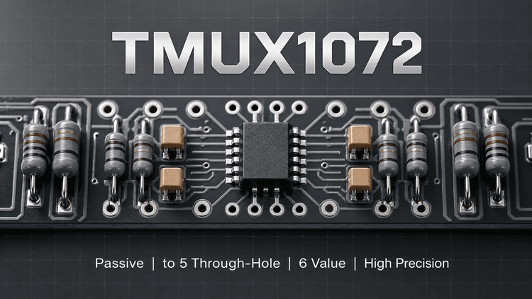
The TMUX1072 is a high-speed, 2-channel (2:1) analog multiplexer designed to handle signal routing beyond the supply rail. It is a bidirectional switch capable of supporting signals up to 5.5 V even when the supply voltage (VCC) is as low as 2.3 V. 💡
Crucially, it integrates Overvoltage Protection (OVP) up to 18 V on common pins and a Fault (FLT) indicator pin. For design engineers, the critical selection variables are its 1.2 GHz bandwidth and 6 Ω On-Resistance (RON), which minimize signal attenuation. For procurement, the Powered-Off Protection (Hi-Z) feature is vital for system safety during power sequencing.
🎯 Typical Applications & Design Context
Based on its 1.2 GHz bandwidth and protection features, the TMUX1072 targets:
- Data Acquisition (DAQ) & Field Instrumentation: Where high-speed signal switching and robust protection against sensor overvoltage are required.
- Video Surveillance & Rear Cameras: The high bandwidth supports signal integrity for SD/eDP video lines or camera data paths.
- HVAC & Industrial Control: The wide temperature range and OVP ensure reliability in harsh environments where external sensors might feed voltages higher than the logic rail.
📊 Key Technical Specifications
Focus on these validated parameters to ensure system compatibility:
| Parameter | Value/Condition | Design Impact |
|---|---|---|
| Supply Range (VCC) | 2.3 V to 5.5 V | Compatible with standard 3.3V and 5V logic rails. |
| Signal Range | Supports signals beyond VCC up to 5.5 V | 📈 Allows routing of higher voltage signals without level shifters. |
| On-Resistance (RON) | 6 Ω (Typical) | Low insertion loss; check if this causes acceptable drop for your load current. |
| Bandwidth (BW) | 1.2 GHz (Typical) | ✨ Suitable for high-speed video and data signals; minimizes capacitive loading. |
| OVP Threshold | 6 V (Detection), 18 V (Protection) | Fault pin triggers at 6V; protection withstands up to 18V on COM pins. |
| Charge Injection (C) | 4.5 pF (Typical) | Low charge injection reduces transient glitches in precision sampling. |
⚠️ Absolute Maximum Ratings & Process Limits
Exceeding these ratings leads to irreversible silicon damage or latent field failures.
| Parameter | Min/Max | Engineering Failure Mode (E-E-A-T Insight) |
|---|---|---|
| Supply Voltage (VCC) | –0.5 V to 6 V | >6V causes immediate oxide breakdown. |
| COM Pin Voltage | –0.5 V to 20 V | While protection exists to 18V, approaching 20V risks latch-up. |
| Continuous Current (VCC/GND) | ±100 mA | 🔒 Overcurrent leads to bond wire fusing or thermal runaway. |
| Junction Temp (TJ) | 150 °C | Exceeding this degrades switching speed and OVP accuracy over time. |
Design Note: While the device has 18V protection, the OVP Detection triggers at approximately 6V. Do not rely on the 18V rating for continuous operation; it is for fault survivability.
🧩 Package, Dimensions & Assembly Notes
- Available Packages: UQFN-12 (2.00mm × 1.70mm) and VSSOP-10 (3.00mm × 5.00mm).
- Thermal & Assembly: The UQFN package utilizes a thermal pad underneath the body.
- SMT Validation: Ensure the PCB landing pattern has proper thermal relief vias connected to GND to dissipate heat during high-frequency switching.
- Inspection: For the UQFN (RUT) package, X-ray inspection is recommended post-reflow to verify voiding under the thermal pad is within IPC standards (e.g., <25%).
- Moisture Sensitivity: Confirm the MSL (usually MSL 3) to ensure proper baking before reflow if the packaging has been open for >168 hours.
🔍 Procurement & Sourcing Insights
- Lifecycle & Supply: As a TI (Texas Instruments) "Production Data" component, it is not NRND (Not Recommended for New Design), but availability varies by package. The VSSOP is often more common than the ultra-small UQFN.
- Alternative Validation: When seeking cross-brands (e.g., Maxim or ON Semi alternatives), verify the Fault Pin logic polarity. The TMUX1072 FLT pin is Active Low Open-Drain. A generic substitute without this specific open-drain architecture will not interface correctly with your microcontroller interrupt without a PCB redesign.
- Market Risk: Given the small footprint of UQFN, counterfeits from unauthorized brokers often have misaligned markings. Procurement must prioritize authorized distribution or utilize XRF material analysis if sourcing is uncertain.
❓ FAQ
Q1: Can I use the TMUX1072 to switch power rails?
A: No. The TMUX1072 is an analog signal switch. While it has 6 Ω RON, it is not designed for high-current power path switching. It is intended for signal lines (Video, SPI, I2C, Analog sensors).
Q2: What happens if the FLT pin is left unconnected?
A: The FLT pin is an Open-Drain output. If unused, the datasheet permits leaving it floating or grounding it. However, if the system logic expects a fault signal, leaving it floating will result in a "High" impedance state, potentially masking an Overvoltage event.
Q3: Does the "Powered-Off Protection" feature protect the downstream MCU?
A: Yes. When VCC = 0 V, the switch enters a Hi-Z state (disconnected). This isolates the MCU inputs from voltage spikes on the COM lines, a critical feature for hot-plugging interfaces like rear cameras or sensor probes.
Q4: Is there a pin-to-pin compatible alternative?
A: Pin-compatible alternatives for UQFN-12 specific multiplexers with integrated OVP are rare. Usually, the package footprint (2.00mm x 1.70mm) is the hardest constraint. If a second source is required, be prepared to redesign the PCB for a different footprint, as the "Thermal Pad" dimensions vary significantly between manufacturers.