📌 Product Overview
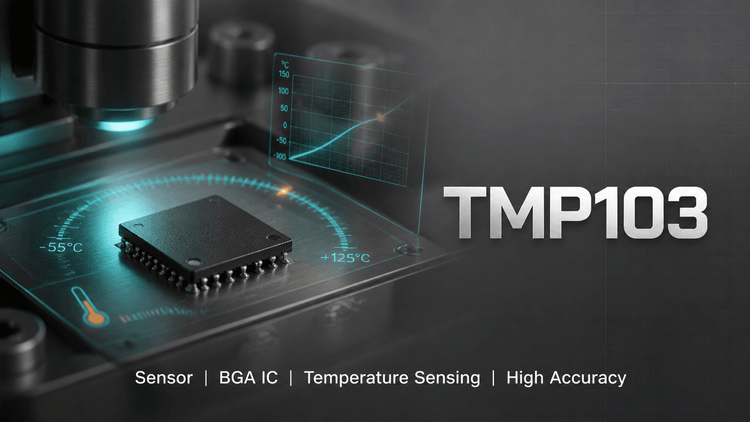
The TMP103 is a miniaturized digital temperature sensor designed by Texas Instruments (TI) in a 4-ball Wafer Chip-Scale Package (DSBGA). With a footprint of only 0.76mm x 0.76mm, it is specifically engineered for space-constrained applications such as smartphones, SSDs, and compact wearables where traditional packaged sensors cannot fit. It utilizes a standard I2C/SMBus interface with 8-bit resolution (1°C) and ±1°C typical accuracy, operating efficiently from 1.4V to 3.6V. For system architects, the TMP103 represents a "zero-real-estate" solution for thermal monitoring in multi-zone high-density boards.
🎯 Typical Applications & Design Context
- Handsets & Wearables: 📱 Ideal for monitoring battery and SoC temperatures due to ultra-low 1µA shutdown current and micro-scale packaging.
- SSD (Solid State Drives): 💾 Critical for thermal throttling protection in tightly spaced M.2 and mSATA form factors where PCB real estate is premium.
- Telecom & Networking: 🌐 Used for monitoring power amplifier (PA) and ASIC temperatures in high-density line cards.
- Industrial/IoT: 🏭 Effective for low-power environmental sensing in remote nodes thanks to the wide voltage range and Multiple Device Access (MDA) support.
This component is chosen not for high-precision metrology, but for density-aware thermal protection in low-power, battery-operated, or tightly packed consumer electronics.
📊 Key Technical Specifications
| Parameter | Value/Condition | Notes |
|---|---|---|
| Supply Voltage | 1.4V to 3.6V | Wide range suitable for single-cell Li-Ion and 1.8V/3.3V logic rails. |
| Temperature Resolution | 8 bits (1°C) | Digital output; no ADC required on host MCU. |
| Accuracy | ±1°C (Typical) | Validated for –10°C to 100°C range. ±2°C Max at 25°C. |
| Interface | I2C / SMBus | Supports standard mode (up to 100kHz). |
| Active Current | 3µA @ 0.25Hz | Extremely low average power consumption. |
| Shutdown Current | 1µA | Minimizes drain on battery when not converting. |
| MDA Feature | Up to 8 devices | 📈 Allows global read/write to multiple sensors on the same bus without individual commands. |
⚠️ Absolute Maximum Ratings & Process Limits
| Parameter | Rating | E-E-A-T Engineering Insight |
|---|---|---|
| Supply Voltage | -0.3V to 4.0V | 🔒 Exceeding 4V or reverse biasing V+ will permanently damage the input ESD structures. During power sequencing, ensure V+ ramps up before or simultaneously with SDA/SCL. |
| Input Voltage (SCL/SDA) | (V+)+0.3V | ⚡ Do not pull up I2C lines to a rail voltage higher than V+. This can cause latch-up or leakage. |
| Junction Temp (Tj) | 150°C | While the ambient spec is 125°C, internal silicon must not exceed 150°C. In SMD reflow, the solder profile peak must be strictly controlled. |
| ESD Rating (HBM) | 2000V | ⚠️ Handling Alert: CDM is only 1000V. Automated handling (tapes, pick-and-place) must be ESD-safe. Manual handling requires wrist straps. |
💡 Failure Mode Note: If the Absolute Maximum Ratings are exceeded during board-level troubleshooting (e.g., using a 5V logic probe on a 1.8V TMP103 bus), the I2C port will likely fail short, blocking the entire bus for other devices.
🧩 Package, Dimensions & Assembly Notes
- Package Type: 4-Ball DSBGA (YFF).
- Body Size: 0.76mm x 0.76mm (Nominal).
- Ball Pitch: 0.4mm.
- Solder Mask Defined (SMD) Pads: The footprint is tiny. PCB designers must strictly follow TI's recommended land pattern (solder mask opening size is critical; too wide causes bridging, too narrow causes poor open yields).
- Assembly Challenge: 👇 Due to the 0.4mm pitch and low profile, X-Ray inspection is mandatory during mass production to verify "Head-in-Pillow" or solder joint alignment, as optical inspection is unreliable.
- Thermal Path: The primary thermal conduction path is through the solder balls into the PCB ground planes. Ensure thermal vias are placed under the GND pad (A2).
🔍 Procurement & Sourcing Insights
- Lifecycle Status: This is a mature but niche component (Released 2011, Revised 2018). It is Not Recommended for New Designs (NRND) in many roadmap contexts, or availability may be limited to specific large Tier-1 customers.
- Supply Chain Risk: ⚠️ The 4-ball DSBGA package is rare in the spot market. Most Huaqiangbei brokers will not have this in stock.
- Counterfeit Risk: 🚨 High. Because the package looks like a simple passive component or "dummy chip," it is a prime target for re-marking or black-top fraud. Always procure through authorized franchised sources.
- Alternative Validation: Replacing the TMP103 requires checking the I2C address mapping. The MDA (Multiple Device Access) feature is a TI-specific extension to standard SMBus. Replacing it with a generic sensor (like NTC or standard IC) requires rewriting the host driver to handle individual addressing.
- MOQ: Typically high MOQ (reel of 3,000-10,000 units) from distribution; sampling may require direct TI support.
❓ FAQ
Q: Can I use the TMP103 on a 5V MCU bus?
A: No. The TMP103 supply voltage (V+) max is 3.6V. Connecting a 5V pull-up resistor on the I2C lines while the sensor is powered at 3.3V may violate the "Voltage at SCL and SDA" absolute rating (V+ + 0.3V), potentially damaging the device. You need a logic level shifter.
Q: What is the "Multiple Device Access (MDA)" and why does it matter?
A: MDA allows the host to send a global read command to up to 8 TMP103 sensors on the same bus simultaneously. This significantly reduces software overhead and bus traffic compared to querying each sensor individually. If you switch to a generic sensor, you lose this efficiency.
Q: Is the 0.76mm DSBGA package hand-solderable?
A: Practically, no. The 0.4mm pitch and micro-scale size make hand soldering extremely difficult and risky for量产. It is designed for high-volume SMT processes with reflow soldering. Prototyping usually requires a breakout board with the sensor pre-soldered.
Q: How do I verify the SMT placement quality?
A: Due to the "hidden" joints under the BGA, X-Ray inspection is the only reliable method to ensure there are no bridging shorts or head-in-pillow defects. Optical cameras cannot see the solder joints adequately.