📌 Product Overview
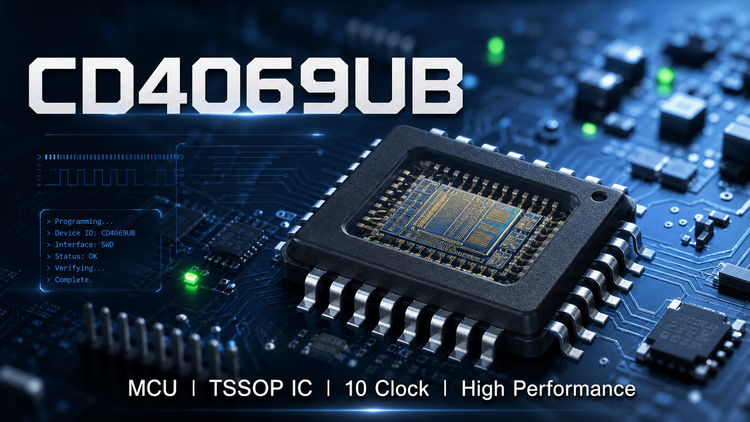
The CD4069UB is a robust, unbuffered Hex Inverter built on CMOS technology, designed for general-purpose logic inversion, signal shaping, and oscillator generation. Unlike buffered counterparts (e.g., CD4049), the unbuffered "UB" architecture allows this device to function effectively as a linear amplifier or low-frequency oscillator, providing critical design flexibility for analog-digital hybrid circuits. For OEMs, the primary selection drivers are its wide supply voltage range (3V to 15V) and standardization across multiple packaging options (PDIP to TSSOP), ensuring compatibility with both legacy maintenance and high-density modern PCB designs.
🎯 Typical Applications & Design Context
Due to its unbuffered design and medium-speed operation, the CD4069UB excels in specific scenarios:
- Crystal Oscillators & Pulse Generators: The high gain and unbuffered input structure enable reliable square-wave generation when combined with a crystal or simple RC network.
- General Logic Level Conversion: Capable of interfacing between varying logic voltage levels (e.g., stepping down 15V CMOS to 5V TTL), provided the current drive requirements are moderate.
- Signal Conditioning: Used for cleaning up noisy waveforms in industrial controls or automotive sensor interfaces where high-speed TTL performance (74HC series) is unnecessary or voltage incompatible.
📊 Key Technical Specifications
| Parameter | Value (Typical @ 10V) | Notes for Engineering |
|---|---|---|
| Supply Voltage (VDD) | 3 V to 15 V | Flexible power rail integration; 3V minimum for battery ops. |
| Propagation Delay (tPLH/tPHL) | 30 ns @ 10V | Defines speed limit; not suitable for high-speed (>10MHz) logic. |
| Quiescent Current (IDD) | 100 nA @ 18V (25°C) | Ultra-low static power; critical for battery-powered designs. |
| Input Current (IIN) | 1 µA @ 18V | High impedance minimizes loading on previous stages. |
💡 Design Note: The "UB" suffix indicates an unbuffered stage. While this enables oscillator use, it increases susceptibility to noise on unused inputs. Unused inputs must be tied to VSS or VDD to prevent oscillation and excessive current draw.
⚠️ Absolute Maximum Ratings & Process Limits
Exceeding these parameters risks immediate silicon failure or latent reliability issues.
| Rating | Maximum Value | Failure Mechanism / Risk |
|---|---|---|
| Supply Voltage (VDD) | –0.5 V to 20 V | Exceeding 20V causes oxide breakdown, leading to permanent short circuits. |
| Input Voltage (VI) | –0.5 V to VDD + 0.5V | Voltages exceeding VDD forward-bias the substrate diode, causing latch-up. |
| Power Dissipation (PD) | 500 mW (Package Dependent) | Thermal runaway; requires derating above 25°C ambient temperature. |
| Lead Temperature (TTL) | 265 °C (10s max) | SMT reflow; exceeding this duration delaminates the package plastic. |
⚠️ E-E-A-T Insight: While the datasheet lists a Max VDD of 20V, sustained operation near this limit significantly increases leakage current. For long-term field reliability, LDeepAI recommends derating supply voltage to a maximum of 85% (16.5V-17V) and ensuring strict input voltage rise times to prevent "mid-supply" conduction states.
🧩 Package, Dimensions & Assembly Notes
The CD4069UB is available in standard leaded and lead-free packages, impacting footprint and SMT profile selection:
- PDIP (CD4069UBE): 19.30mm x 6.35mm. Through-hole legacy support.
- SOIC (CD4069UBM): 8.65mm x 3.91mm. The industry standard for automated SMT placement.
- TSSOP (CD4069UBPW): 5.00mm x 4.40mm. Ideal for space-constrained handheld designs.
- SMT Validation: All surface-mount variants (M/NSR/PW) are moisture-sensitive. If the MSL rating (typically 3) is exceeded prior to reflow, internal "popcorning" cracks will occur.
- Pad Design: Ensure the thermal pad (if present on center pad variants) is soldered to the ground plane to assist heat dissipation, although power dissipation is low compared to MCUs.
🔍 Procurement & Sourcing Insights
Sourcing the CD4069UB requires navigating a mature but fragmented supply chain:
- Supply Volatility: While categorized as "Standard Logic," specific package variants (particularly the TSSOP or Ceramic CDIP) often face erratic lead times extending to 20+ weeks depending on the major manufacturer (TI, ON Semi, ST).
- Authenticity Risks: This is a high-risk part for "remarking" in the open market. Scratched-off date codes or inconsistent laser marking etching often indicate pulled or recycled components, common in Huaqiangbei spot markets.
- Alternative Strategy: Pin-to-pin replacements are generally reliable among major brands (e.g., TI CD4069UBM vs. NXP HEF4069UB). However, always validate the "UB" (Unbuffered) distinction. Substituting with a buffered "B" version (e.g., CD4069B) will fail oscillator circuits.
- LDeepAI Recommendation: Secure authorized stock for prototypes to establish the "Golden Reference." For mass production, consider allocating 5-10% buffer stock for this low-cost but high-volume component to avoid line stoppages.
❓ FAQ
Q: Can I replace a CD4069UB with a 74HC04 directly?
A: No. The 74HC04 is a High-speed CMOS device limited to ~2V-6V supply. The CD4069UB handles up to 15V (sometimes 18V). Using a 74HC04 in a 12V industrial application will result in immediate failure. Furthermore, the input thresholds of HC families are different.
Q: Why does my oscillator circuit fail with a generic 4069?
A: You likely used a Buffered 4069 (sometimes labeled just CD4069B) instead of the Unbuffered CD4069UB. Buffered stages have square transfer characteristics and lack the linear gain region required for crystal oscillation.
Q: What is the lead time for the TSSOP package (CD4069UBPW)?
A: The TSSOP package is less common than the SOIC. Lead times from franchised distributors often fluctuate between 12-24 weeks. We recommend checking the PDIP/SOIC alternatives for faster availability if PCB space permits.
Q: Do unused inputs float safely?
A: Never. Floating inputs on CMOS devices can float to mid-voltage, turning on both PMOS and NMOS transistors simultaneously. This causes drastic shoot-through current (heating) and erratic output behavior. Tie all unused inputs to Ground or VDD.