📌 Product Overview
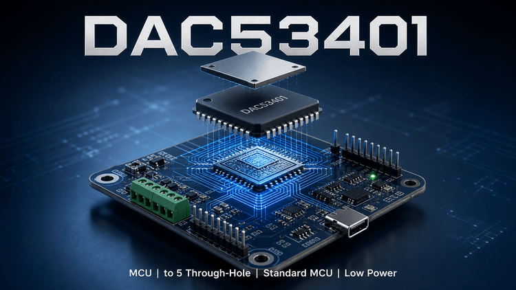
The DAC53401 is a 10-bit, voltage-output Digital-to-Analog Converter (DAC) featuring a PMBus-compatible I2C interface and Nonvolatile Memory (NVM). Housed in a tiny 2mm × 2mm WSON (8-pin) package, it integrates an internal reference and LDO, designed to minimize board space while maximizing control precision. 🔬
For engineering teams, the critical selection variables are the wide supply range (1.8V to 5.5V) and the internal feedback pin (FB), which allows the device to function as a programmable voltage regulator or margining controller. It is optimized for applications requiring low power consumption (0.2mA at 1.8V) and high-density mounting.
🎯 Typical Applications & Design Context
Based on its feature set—specifically the internal feedback, PMBus interface, and tiny footprint—the DAC53401 fits into high-precision control loops rather than simple signal generation.
- Power Supply Margining: 💡 Using the FB pin, engineers can dynamically adjust DC/DC converter output voltages for server rack validation (VRM 13.0 compliant).
- LED Biasing & Calibration: Suited for optical modules where PWM-to-Voltage conversion is required for automatic power control (APC) loops in active antenna systems (mMIMO).
- Medical Alarms: The pre-programmable waveform generator (square/sawtooth) supports priority tone generation without MCU overhead.
📊 Key Technical Specifications
| Parameter | Specification | Design Impact |
|---|---|---|
| Resolution | 10-bit (DAC53401) | ~1024 steps; enables precise voltage margining (±0.1% typical). |
| Output Range | 0V to VDD | VDD is the reference; requires a clean, low-noise supply for signal integrity. |
| Interface | I2C (PMBus compatible) | Supports Standard/Fast/Fast+ modes; simplifies integration into management buses. |
| Startup Behavior | Hi-Z or 10k-GND | NVM recalls settings; prevents voltage spikes during system power-on (POR). |
| I/O Supply | 1.8V to 5.5V | High flexibility; allows direct connection to 3.3V MCUs or 5V rail logic. |
⚠️ Absolute Maximum Ratings & Process Limits
Exceeding these ratings causes latent failure or immediate silicon damage.
| Parameter | Rating | 🔥 Failure Mechanism |
|---|---|---|
| VDD (Supply) | -0.3V to +6.0V | >6V permanently damages the ESD structures and input LDO. |
| Analog Input (FB) | -0.3V to VDD + 0.3V | If FB voltage exceeds VDD during transients, parasitic latch-up may occur. |
| Junction Temp (Tj) | 150°C | Exceeding this causes thermal runaway in the WSON package. |
| ESD Rating | HBM 2kV, CDM 500V | Sensitive component; requires proper grounding during handling. |
🚨 E-E-A-T Insight:
The CAP pin (Pin 4) requires an external capacitor (0.5µF to 15µF) to AGND. Do not leave this floating. Failure to place this capacitor results in internal LDO instability, causing oscillation on the VDD line and corrupting the analog output. This is a common "No-Fault-Found" issue in bring-up.
🧩 Package, Dimensions & Assembly Notes
- Package Type:WSON (8-pin), 2.00mm × 2.00mm Nominal Body Size.
- Thermal Pad: The device features a thermal pad (exposed die attach pad) on the bottom. This must be soldered to the PCB ground plane for heat dissipation.
- SMT Reflow: Recommended profile follows standard SnAgCu (SAC) reflow (Peak 245°C).
- Stencil Design: Ensure proper aperture ratio for the center thermal pad to avoid tombstoning or voiding. A 1:1 opening ratio for the center pad is recommended for adequate paste volume.
🔍 Procurement & Sourcing Insights
- Lifecycle Status: The datasheet indicates "Production Data" (Active), not "Advanced Information". This implies mature tooling and stable supply, but obsolescence risks should be monitored annually.
- Pin Compatibility: The DAC43401 (8-bit) is pin-to-pin compatible. If cost is the driver, the 8-bit version can be substituted, but software gain compensation is required for the same LSB size.
- Supply Chain Risk: Being a Texas Instruments (TI) component, Huaqiangbei markets may stock factory surplus or "pulls" (reclaimed parts).
- ⚠️ Risk: Reclaimed WSON packages are highly susceptible to lead finish oxidation or thermal pad damage from prior removal, leading to solderability failures.
- Strategy: Verify traceability codes (Date Code/Lot) on the reel. Avoid "loose" or "cut tape" supplies for mass production.
❓ FAQ
Q: Can I use the DAC53401 to drive a LED directly?
A: No. The OUT pin is a voltage-output DAC with limited current drive (buffered). To drive an LED, you must use the DAC output to drive the REF/ADJ pin of an external LED driver IC, or use a simple BJT/MOSFET circuit. Do not sink LED current directly into the DAC output.
Q: What is the difference between Hi-Z and 10k-GND startup modes?
A: This determines the state of the DAC output before the I2C interface initializes. Hi-Z (High Impedance) leaves the output floating (safe for shared lines). 10k-GND actively pulls the output to ground via a 10kΩ resistor. For power supply margining, 10k-GND ensures the rail stays at 0V until commanded to rise, preventing overshoot.
Q: Is the CAP pin capacitor value critical?
A: Yes. It stabilizes the internal LDO. While the range is 0.5µF to 15µF, 1µF ceramic (X7R) is the industry standard choice. Placing it too far from the pin (>5mm trace length) negates its effect.
Q: How does the A0 pin addressing work?
A: Pin 1 (A0) is a 4-state address input. By connecting it to VDD, GND, SDA, or SCL, you can create up to 4 unique I2C addresses on a single bus. This allows stacking 4 DACs on one control line without address collision.