📌 Product Overview
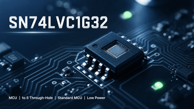
The SN74LVC1G32 is a single 2-input positive-OR gate from the LVC (Low-Voltage CMOS) family, designed for 1.65V to 5.5V operation. It performs the Boolean function Y = A + B in positive logic. This device is ideal for space-constrained PCBs requiring logic level translation, signal gating, or generic Boolean functions. With its ultra-small 0.8mm² X2SON package option and wide voltage support, it serves as a critical glue logic component in mixed-voltage systems, portable electronics, and high-density industrial controllers.
🎯 Typical Applications & Design Context
💡 Signal Level Translation: Designed for interfacing between different logic voltage levels (e.g., 1.8V MCU to 3.3V Sensor), thanks to inputs accepting voltages up to 5.5V.
🚀 Consumer Portables: Used in AV receivers, Blu-ray players, and GPS units where board space and power budget (10µA max Icc) are premium.
🏭 Industrial Networking: Deployed in telecom power distribution units (PDUs) and wireless infrastructure for battery monitoring and signal conditioning.
⚡ Power Management: Supports live insertion and partial-power-down modes, making it suitable for hot-swap server PSU and RAID controller designs.
📊 Key Technical Specifications
| Parameter | Value/Condition | Engineering Note |
|---|---|---|
| Voltage Range (VCC) | 1.65 V – 5.5 V | Flexible supply rail for battery and 3.3V/5V logic |
| Propagation Delay (tpd) | 3.6 ns (Max) @ 3.3V | High-speed operation for signal gating without bottleneck |
| Output Drive | ±24 mA @ 3.3V | Strong drive capability for short trace transmission lines |
| Static Power (Icc) | 10 µA (Max) | Ultra-low power consumption for battery-powered devices |
| Input Levels | Vt compatible | Supports down-translation to VCC |
| Logic Function | Y = A + B | Positive-OR Gate |
⚠️ Absolute Maximum Ratings & Process Limits
| Parameter | Limit | 🔒 E-E-A-T Failure Analysis |
|---|---|---|
| Supply Voltage (VCC) | -0.5 V to 6.5 V | Exceeding 6.5V risks immediate gate oxide breakdown. |
| Input Voltage (VI) | -0.5 V to 6.5 V | Voltages > VCC + 0.5V can trigger latch-up or cause CMOS SCR structures to fire. |
| Continuous Output Current | ±50 mA | Current > 50mA (even pulsed) exceeds metallization fusing current. PCB traces will act as fuses, vaporizing copper. |
| Operating Tj | -40°C to 125°C | Beyond 125°C, timing parameters degrade (tpd increases), risking logic setup/hold violations. |
| Storage Temp (Tstg) | -65°C to 150°C | Moisture ingress occurs if stored >150°C; requires baking if MSL >3. |
🧩 Package, Dimensions & Assembly Notes
📦 Form Factor Availability:
- X2SON (DPW): 0.8mm × 0.8mm (Body), 0.5mm pitch. The smallest form factor, demanding high-precision stencil design (laser-cut stainless steel recommended) and advanced inspection (AOI/X-ray) for bridging.
- DSBGA (YZP): 1.38mm × 0.88mm. Requires underfill for mechanical reliability in vibration environments.
- SOT-23 (DBV): 2.90mm × 2.80mm. Standard, manual assembly friendly.
⚠️ SMT Validation:
The 0.5mm pitch on the X2SON package is highly sensitive to tombstoning during reflow. Ensure a balanced thermal pad layout on the PCB and use nitrogen-rich reflow profiles to minimize wetting skew.
🔍 Procurement & Sourcing Insights
🔍 Alternative Evaluation:
While logic gates are often considered "commodities," the LVC family differs from HC/AUC families in threshold voltage (Vt). Substituting with an SN74AUC1G32 (designed for 0.8V~2.7V) into a 3.3V rail will result in non-functional logic. Cross-reference must strictly match the "LVC" designation.
🚢 Supply Chain Status:
This is a high-runner, mature TI part. Lead times are generally stable (0-6 weeks). However, specific micro-packages (DSBGA/X2SON) are often manufactured on dedicated lines; in shortage scenarios, larger packages (SOT-23) are easier to source.
🛡️ Counterfeit Watch:
Common failure modes in the open market involve remarked 74HC series parts sold as 74LVC. Electrical validation of VCC (down to 1.65V) is mandatory to detect fraud.
❓ FAQ
Q: Can I replace SN74LVC1G32 with SN74HC1G32?
A: No. The 74HC family does not support 1.65V operation; its minimum VCC is typically 2V. Using HC in a 1.8V design will result in logic failure.
Q: What is the risk of using the X2SON (0.8mm body) package?
A: The primary risk is solder joint inspection. The thermal pad is underneath the chip. Without X-ray or advanced AOI, opens (insufficient solder) are invisible. This package is not recommended for low-cost CM assembly lines without X-ray verification.
Q: Does this part support 5V inputs when running at 3.3V VCC?
A: Yes. The SN74LVC1G32 inputs are 5V tolerant. You can feed a 5V signal into the input while the device is powered by 3.3V, providing robust translation without clamp diode issues.
Q: How critical is the ESD rating on this tiny part?
A: Very. The datasheet cites 2000V HBM. During manual handling or unautomated kitting, the tiny X2SON/DSBGA packages lack protective spacing. Grounded wrist straps and ionizers are mandatory on the production line to prevent latent yield defects.