📌 Product Overview
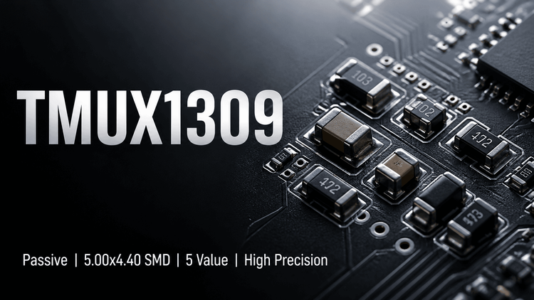
The TMUX1309 from Texas Instruments is a 4:1, 2-channel (differential) bidirectional multiplexer designed for general-purpose analog and digital switching. Unlike standard legacy switches, it integrates Injection Current Control and eliminates the internal ESD diode path to VDD, removing the risk of back-powering the supply rail. Targeting Data Center Switches, Rack Servers, and Industrial Automation, it serves as a robust, pin-compatible upgrade for industry-standard 4052/4852 multiplexers, offering rail-to-rail operation and Fail-Safe logic protection.
🎯 Typical Applications & Design Context
This component excels in environments where signal integrity and power-up sequence control are critical.
- Data Center & Telecom: Used for rack server diagnostics and Remote Radio Units (RRU) due to high off-isolation and low crosstalk.
- Industrial Monitoring: Ideal for electricity metering and appliance control (e.g., air conditioners) where wide supply range (1.62V to 5.5V) simplifies mixed-voltage system design.
- Differential Signal Routing: The dual 4:1 (differential) architecture makes it suitable for multiplexing sensor pairs or low-speed differential lines in space-constrained designs.
📊 Key Technical Specifications
| Parameter | Value/Condition | Design Impact |
|---|---|---|
| Supply Range | 1.62 V to 5.5 V | ✅ Ensures compatibility with both 1.8V and 3.3V/5V logic without level translators. |
| On-Resistance (RON) | 9.5 Ω (Typical) | ⚡ Low insertion loss suitable for signal paths without significant voltage drop. |
| Logic Input | 1.8 V Compatible | ✅ Can be driven directly by low-voltage MCUs/FPGAs. |
| Bandwidth (-3dB) | 270 MHz (Typ) | 🚀 Sufficient for high-speed digital signal multiplexing and video switching. |
| Charge Injection | 0.5 pC (Typ) | 🎯 Minimizes glitching on the output channel during switching, critical for precision measurement. |
⚠️ Absolute Maximum Ratings & Process Limits
Strict adherence to these ratings is required to prevent latent failure or immediate damage during SMT and operation.
| Rating | Symbol | Limit | Failure Consequence (E-E-A-T Insight) |
|---|---|---|---|
| Analog Voltage Range | VSx, VDx | -0.5 V to +5.5 V | 💥 Exceeding -0.5V forward-biases internal ESD structures, potentially causing latch-up or permanent IC damage if ground bounce occurs. |
| Supply Voltage | VDD | -0.5 V to +5.5 V | 🔥 Over-voltage destroys the CMOS structure; the lack of a VDD diode offers no protection against positive surges. |
| Continuous Current | IDK (per pin) | ±20 mA | 📉 Current exceeding this limit fuses the trace, disconnecting the channel permanently. |
| Operating Temp | TA | -40°C to +125°C | 🌡️ Junction temperature limits: With high RON, power dissipation (I2R) requires thermal derating in high-temp ambient environments like outdoor RRUs. |
🧩 Package, Dimensions & Assembly Notes
- Available Packages: PW (TSSOP-16: 5.00x4.40mm), DYY (SOT-23-THIN-16: 4.20x2.00mm), BQB (WQFN-16: 3.50x2.50mm).
- Soldering & Layout: For the WQFN (BQB) package, the center thermal pad must be soldered to the PCB ground plane for heat dissipation.
- Alternative Note: 💡 The DYY (SOT-23-THIN) is an ideal drop-in replacement for legacy 4052 designs where PCB real estate is constrained, offering a significantly smaller footprint than TSSOP.
🔍 Procurement & Sourcing Insights
- Supply Chain Stability: TI's "Functional Safety-Capable" classification makes this a long-lifecycle industrial part, reducing obsolescence risk compared to consumer-grade multiplexers.
- Replacement Logic: Verify Pin Compatibility (Pin-to-Pin) with legacy CD4052B or TS5A3159. While pin-maps align, the TMUX1309 requires clean power sequencing; it lacks the legacy diode path, meaning "floating" VDD boards behave differently than with old 4000-series logic.
- Sourcing Vigilance: 🚨 Beware of "Green" or counterfeits in open market channels; verify the "Injection Current Control" parameter in incoming QC, as recycled units often fail here due to internal ESD degradation.
❓ FAQ
Q: Can I use the TMUX1309 to switch power rails?
A: No. The TMUX1309 is optimized for signal switching (max 20mA continuous current per pin). It lacks the current handling capability and thermal mass of a power load switch. Using it for power distribution risks thermal shutdown or bond-wire failure.
Q: Is the TMUX1309 a direct drop-in replacement for the CD74HC4052?
A: Electrically yes, but validate your supply startup sequence. The TMUX1309 features "Fail-Safe Logic," allowing control signals (VLOGIC) before VDD is stable. Legacy HC4052 might float outputs during this state; the TMUX1309 keeps them disabled, which prevents unexpected glitches but requires confirming your logic drivers expect this behavior.
Q: What does "Injection Current Control" mean for my PCB layout?
A: It means you can remove the external Schottky diodes and series resistors you typically place on signal lines to protect the switch from overvoltage. The TMUX1309 handles signals above VDD internally (up to max rating), simplifying your BOM and PCB routing.
Q: Why did my predecessor specify a WQFN package over TSSOP?
A: Likely for thermal density or board space. The WQFN (3.5x2.5mm) is significantly smaller than TSSOP. However, the WQFN requires X-Ray inspection for BGA verification or careful thermal pad soldering design, whereas TSSOP is visibly inspectable. Choose based on your assembly line's optical inspection capabilities.