📌 Product Overview
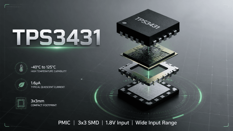
The TPS3431 is a standard programmable watchdog timer designed to enhance system reliability in microcontroller-based applications. 💡 Targeting sectors like industrial asset tracking, energy storage systems, and surgical equipment, this component serves as a critical "last line of defense" against software lock-ups. Unlike simple reset ICs, it offers a balance of programmability and precision, allowing engineers to tailor the watchdog window (WDT) via an external capacitor or factory presets. For R&D teams, the primary selection variable is the timing accuracy across temperature—±2.5% at 25°C—ensuring the watchdog doesn't falsely trigger a reset during legitimate extended processing times, a crucial factor for battery-powered or remote industrial devices.
🎯 Typical Applications & Design Context
The TPS3431 is ideally suited for applications requiring high availability and low power consumption. Its low quiescent current (10 µA typical) and wide input voltage range (1.8 V to 6.5 V) make it a robust choice for:
- Cellular Asset Trackers: Ensures the module resets from deadlocks without draining the battery.
- Energy Storage PCS: Maintains watchdog supervision in power conversion subsystems where voltage fluctuations are common.
- Medical & Industrial Equipment: Provides a safety layer for IP cameras and surgical tools, utilizing the Wide VDD range to interface seamlessly with diverse logic levels (3.3 V or 5 V).
📊 Key Technical Specifications
| Parameter | Specification | Engineering Impact |
|---|---|---|
| Input Voltage (VDD) | 1.8 V to 6.5 V | 👉 Wide Compatibility: Supports direct connection to both 3.3V and 5V MCU rails without extra LDOs. |
| Watchdog Accuracy | ±2.5% (25°C) | 💡 Precision: Prevents nuisance tripping in systems with tight timing tolerances. |
| Quiescent Current | 10 µA (Typical) | 🔋 Low Power: Essential for always-on battery applications; minimizes standby drain. |
| Output Type | Active-low Open-Drain | 📉 Flexibility: Allows wired-OR configuration and level shifting to different MCU logic voltages. |
| Operating Temp | –40°C to +125°C | 🌡️ Industrial Grade: Suitable for harsh environments and outdoor automotive/industrial deployments. |
⚠️ Absolute Maximum Ratings & Process Limits
| Rating | Value | E-E-A-T Validation Insight |
|---|---|---|
| Supply Voltage | –0.3 V to 7 V | 🚨 Input Protection: Exceeding 7V, even during surge transients in industrial environments, can cause permanent gate oxide damage. Designers must ensure input transient suppression (TVS) clamps below this threshold. |
| Junction Temp (Tj) | 150°C | ⚠️ Thermal Derating: The 3x3mm VSON package relies on PCB copper pours for heat dissipation. High ambient temperatures combined with supply voltage near 6.5V necessitate careful thermal simulation to avoid thermal shutdown. |
| ESD Rating | 2kV (HBM) | 🛡️ Handling Risk: While robust, the small VSON pins are susceptible to ESD during manual handling if proper ground straps are not used during prototyping. |
Failure Analysis Note: Exceeding the Absolute Maximum Rating on the CWD pin, even briefly with a fast spike (e.g., from a nearby inductive switching node), can degrade the internal capacitor charge pump or pin isolation, leading to a permanent shift in watchdog timing accuracy.
🧩 Package, Dimensions & Assembly Notes
The TPS3431 is housed in a 3.00 mm × 3.00 mm VSON-8 (Very-thin Small Outline No-lead) package.
- PCB Design: The package features a thermal pad (exposed pad) on the bottom. For mass production reliability, this pad must be soldered to the PCB ground plane. 👇 Soldering this pad is not optional; it provides the primary mechanical anchor and thermal path.
- SMT Validation: The VSON footprint requires a "solder paste stencil window reduction" (typically 50-60% of the pad area for the thermal pad) to prevent solder wicking or voiding. X-ray inspection (3D X-ray) is recommended during NPI (New Product Introduction) to verify voiding is below IPC Class 2 standards.
- Layout Sensitivity: Keep the CWD trace short. Long traces to the programming capacitor can introduce noise, falsely triggering the watchdog or extending the timeout period unintentionally.
🔍 Procurement & Sourcing Insights
- Lifecycle Stability: As a mature TI product (released 2018, revised 2021), the TPS3431 is generally in stable production, but allocation is common for specific TI Watchdog families.
- Alternative Evaluation: When evaluating second sources (e.g., Maxim/ADI or ROHM equivalents), cross-reference the EN (Enable) logic carefully. The TPS3431 has an internal pull-up; some competitors require an external logic state to function.
- Supply Chain Risks: ⚠️ Watchdog Timing Mismatch: Ensure the distributor-provided date codes are fresh. Ceramic capacitors (used for CWD) can drift with age/humidity, but the IC itself should not exhibit "parametric drift" if sourced from authorized channels.
- BOM Cost: The external capacitor requirement adds a BOM line item. Consider the total landed cost (IC + Capacitor) vs. fully integrated watchdogs to ensure cost targets are met.
❓ FAQ
Q: Can I leave the Enable (EN) pin floating?
A: Yes. 👍 The datasheet confirms the EN pin has an internal pull-up to VDD. Leaving it floating (NC) enables the watchdog function by default. Grounding this pin is the standard method to disable the watchdog during firmware development or testing.
Q: What is the difference between using the CWD pin vs. Factory Settings?
A: The CWD pin allows custom timing via an external capacitor ($t_{WD} \propto C_{WD}$). If you leave CWD open or tied to VDD via 10k$\Omega$, the device defaults to factory-programmed timeouts. 👉 Use CWD for unique timing requirements; use internal settings to save PCB space and component cost.
Q: How does the Open-Drain output affect my reset circuit design?
A: The WDO (Watchdog Output) is an open-drain NMOS. It requires a pull-up resistor to the MCU's logic voltage (e.g., 3.3V). 💡 This allows you to safely connect the TPS3431 (powered by 5V) to a 3.3V MCU without level shifters, provided the pull-up is referenced to 3.3V.
Q: Why did my board fail thermal validation?
A: The VSON-8 package is small. If your input voltage is 6.5V and the ambient temperature is high (>85°C), the power dissipation (though low, ~0.065W) may spike the junction temperature without sufficient PCB copper underneath the thermal pad. Verify your thermal relief patterns.