📌 Product Overview
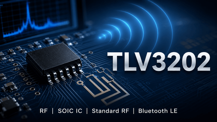
The TLV3202 is a dual-channel, precision comparator designed by Texas Instruments to bridge the gap between high-speed response and ultra-low power consumption. 👉 It features a fast 40ns propagation delay while maintaining a low quiescent current of 40µA per channel, making it ideal for battery-powered and industrial sensing applications.
🏭 Target Applications:
Engineers typically select this component for inspection equipment, high-speed sampling systems, and portable communications where space and power are constrained. 💡 The device offers a push-pull output stage capable of driving significant loads without requiring external pull-up resistors, simplifying PCB layout.
🎯 Typical Applications & Design Context
⚡ Why it fits these scenarios:
Due to its microPOWER architecture and rail-to-rail input capability, the TLV3202 excels in environments where signal integrity must be maintained near the ground and supply rails.
- High-Speed Sampling Systems: The 40ns propagation delay ensures rapid detection of threshold crossings, essential for waveform shaping and PWM edge detection in mixed-signal systems.
- Industrial Threshold Detection: With an extended industrial temperature range (-40°C to 125°C) and low input offset voltage (1mV), it provides reliable switching performance in harsh environments like factory automation.
- Portable Telecom: The low supply current (40µA) minimizes battery drain in handheld devices without sacrificing the speed required for data packet handling.
📊 Key Technical Specifications
| Parameter | Value | Condition / Note |
|---|---|---|
| Propagation Delay | 40ns | High-speed response time (tpd) |
| Supply Voltage Range | 2.7V to 5.5V | Flexible for 3.3V and 5V systems |
| Quiescent Current | 40µA/ch | Low power consumption (microPOWER) |
| Input Offset Voltage | 1mV (Typ) | High precision threshold detection |
| Input Common-Mode | Extends 200mV beyond rails | Allows sensing near GND/VCC |
| Output Type | Push-Pull | Drives loads directly; no pull-up needed |
⚠️ Absolute Maximum Ratings & Process Limits
Understanding the "breaking points" is critical for mass production reliability.
| Parameter | Rating | Failure Mode (E-E-A-T Insight) |
|---|---|---|
| Supply Voltage | 7V (Max) | Exceeding this causes immediate oxide breakdown of the input stage, destroying the ESD protection. |
| Differential Input | ±VCC | If the voltage between IN+ and IN- exceeds the supply, parasitic transistors latch, causing erratic output behavior or permanent damage. |
| Operating Temp | -40°C to 125°C | Industrial grade. ⚠️ At 125°C, thermal derating is required for high output currents to prevent package melting (VSSOP) or thermal shutdown. |
| Output Current | Limited by Junction Temp | Shorting the output to GND while high can exceed the power dissipation limit, leading to bond wire fusing. |
💡 Process Note: While the datasheet specifies "Push-Pull," engineers must ensure the load capacitance does not exceed the recommended limit, or oscillation (ringing) may occur during the fast 40ns switching transition.
🧩 Package, Dimensions & Assembly Notes
The TLV3202 is available in two distinct surface-mount packages optimized for different density levels:
VSSOP (8-Pin):
- Body Size: 3.00mm × 3.00mm
- Pitch: 0.65mm
- Assembly: Requires precise stencil alignment; suitable for automated optical inspection (AOI) due to exposed pad (if applicable) or lead visibility.
SOIC (8-Pin):
- Body Size: 4.90mm × 3.91mm
- Pitch: 1.27mm
- Assembly: Standard assembly process. Easier for manual rework/prototyping compared to VSSOP.
🚫 SMT Warning: During reflow soldering, the thermal profile must respect the maximum body temperature rating. Although small, the high power dissipation capability implies thermal relief pads are recommended for the VSSOP package to dissipate heat during fast switching.
🔍 Procurement & Sourcing Insights
- Supply Chain Stability: As a long-lifecycle TI component, the TLV3202 is generally stable, but specific package codes (e.g., VSSOP vs. SOIC) may have divergent lead times. Always verify the specific suffix (e.g., TLV3202ID vs. TLV3202DGK).
- Risk Factor: Common in the "Gray Market" as removed parts from scrap boards.
- Authenticity Verification: Check for inconsistent laser marking font on the top side of the package.
- Alternative Strategy: If allocation occurs, the LMV7235 is a listed alternative with slower speed (75ns) but similar footprint in some packages. Do not substitute with Open-Drain comparators (like the LMV7235 variant) without checking PCB pull-up resistors, as the TLV3202 has a Push-Pull output.
❓ FAQ
Q: Can I replace the TLV3202 with a cheaper open-drain comparator if I find one?
A: ❌ Risky. The TLV3202 has a Push-Pull output. If you substitute it with an Open-Drain comparator (like the TLV3011/TLV3012 mentioned in the comparison table), your output will be Low only. The High state relies on a pull-up resistor. Without modifying your PCB to add pull-up resistors, the system will fail to read logic High.
Q: What is the most common failure mode during SMT assembly?
A: Cold Solder Joints on VSSOP pins. Due to the 0.65mm pitch, insufficient solder paste volume or misalignment can lead to opens on the input pins, resulting in "floating" comparator outputs that read random noise. Ensure 3D AOI inspection covers the heel fillets.
Q: The datasheet mentions inputs extend 200mV beyond rails. Does this apply to both 3.3V and 5V supplies?
A: ✅ Yes. The Common-Mode Range allows inputs to exceed VCC by 200mV (e.g., sensing 5.2V signals while powered at 5V). However, be careful with Differential Voltage limits. Never force one input to 5.5V and the other to 0V if VCC is only 3.3V, as the differential voltage may exceed the absolute maximum rating (±VCC).
Q: Is the "40ns" propagation delay affected by temperature?
A: 📈 Yes. Propagation delay typically increases as temperature drops. While 40ns is specified at room temperature, you should budget for an additional 10-20ns delay at -40°C for timing-critical designs to ensure the switching threshold is met in cold environments.