📌 Product Overview
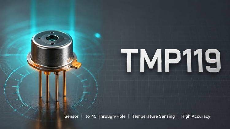
The TMP119 from Texas Instruments is an ultra-high-accuracy, low-power digital temperature sensor with an I2C/SMBus-compatible interface, supplied in a 6-bump DSBGA (YBG) package measuring just 0.95mm × 1.488mm. It delivers 16-bit resolution (0.0078°C/LSB) with ±0.08°C maximum accuracy from 0°C to 45°C — calibration-free.
💡 It is designed to help meet ASTM E1112 and ISO 80601-2-56 medical thermometer requirements, and can directly replace Class AA PT100/PT500/PT1000 platinum RTDs, eliminating precision references, matched traces, and calibration circuits.
Selection-critical variables: accuracy window by temperature range, 4-device bus limit, supply range (1.7–5.5V), and DSBGA assembly process capability.
🎯 Typical Applications & Design Context
- Electronic patient thermometers — accuracy profile engineered to ASTM E1112 / ISO 80601-2-56 without factory calibration
- RTD replacement (PT100/PT500/PT1000) — Class AA-comparable accuracy at a fraction of PT100 excitation power; no ADC reference or linearization algorithm needed
- Cold chain asset tracking & wireless environmental sensors — 3.5µA at 1Hz, 150nA shutdown extends battery life dramatically
- Wearables, thermostats, heat/gas meters, temperature transmitters — strain-tolerant design survives molding, underfill, and board flexing
📊 Key Technical Specifications
| Parameter | Value |
|---|---|
| Accuracy (0°C to 45°C) | ±0.08°C (max), ±0.03°C (typ) |
| Accuracy (–40°C to 85°C) | ±0.12°C (max) |
| Accuracy (–55°C to 150°C) | ±0.2°C (max) |
| Resolution | 16-bit, 0.0078°C (1 LSB) |
| Operating range | –55°C to 150°C |
| Supply voltage | 1.7–5.5V (–55°C to 70°C); 1.8–5.5V (to 150°C) |
| Current @ 1Hz | 3.5µA avg; 135µA active; 150nA shutdown |
| Interface | I2C / SMBus, up to 4 devices per bus |
| Non-volatile memory | Integrated EEPROM + 48 general-purpose bits |
| NIST traceability | 100% production test, ISO/IEC 17025-verified |
⚠️ Absolute Maximum Ratings & Process Limits
🔒 Key boundaries confirmed or inferred from the datasheet structure:
| Limit | Condition |
|---|---|
| Supply range | 1.7–5.5V full function; note the 1.8V minimum above 70°C — a 100mV margin trap in thermally coupled designs |
| Temperature exposure | –55°C to 150°C (accuracy degrades to ±0.2°C max) |
| Soldering/strain | Strain tolerant (soldering, molding, underfill, board flex) — but DSBGA bump stress still depends on board stiffness |
💡 E-E-A-T reality check: ±0.08°C is a die-level spec. In mass production, self-heating from poor thermal layout, board flex stress during depaneling, and reflow profile overshoot on a 6-bump DSBGA are the top three causes of field accuracy drift. Validate with in-situ reference comparison, not just bench samples — SMT yield on sub-1.5mm DSBGA packages typically requires a qualified profile and X-ray or AOI coverage of bump joints.
🧩 Package, Dimensions & Assembly Notes
| Item | Detail |
|---|---|
| Package | YBG, DSBGA, 6 bumps |
| Body size | 0.95mm × 1.488mm (including bumps) |
| Assembly | Standard SnPb-free reflow; DSBGA requires accurate pad design, solder mask opening control, and a stable reflow profile |
| Placement | Package is small and light — verify nozzle compatibility on high-speed placement machines |
🚀 Design note: the strain tolerance claim reduces (not eliminates) sensitivity to PCB warpage. For molding or underfill processes, run first-article accuracy verification across a temperature sweep, since mechanical coupling can shift readings by tens of millikelvin on high-precision dies.
🔍 Procurement & Sourcing Insights
- 👇 Lifecycle & availability: New 2024 device (SNIS236); recent TI introduction means allocation risk is low now but sample-to-production lead time should be locked early for medical programs with long qualification cycles.
- Alternative mapping: TMP117 family (±0.1°C/±0.05°C variants) shares the 1.7–5.5V supply and interface architecture but differs in accuracy grade and register behavior — verify firmware compatibility before drop-in substitution.
- Traceability: Datasheet claims NIST traceability and ISO/IEC 17025 calibration — insist on TI-franchised or authorized channel with date-code and lot documentation; Huaqiangbei gray-market DSBGA parts are effectively impossible to visually authenticate at 0.95mm scale.
- LDeepAI can support sample requests, MOQ quotation, and TMP117/TMP119 cross-variant availability checks — reach out for validated sourcing options.
❓ FAQ
Q: Can the TMP119 directly replace a PT100 RTD system?
A: Yes — TI positions it as a single-chip Class AA RTD alternative, removing the precision excitation reference, matched traces, and linearization calibration. Confirm your system accepts a digital I2C output rather than an analog resistance signal.
Q: How many TMP119 devices fit on one bus?
A: Four, via address pins/configuration. Plan address assignment early if you need more sensing points.
Q: What's the biggest accuracy trap in production?
A: Self-heating and board-level stress. The ±0.08°C spec assumes minimal heat transfer from the PCB; thermal vias, nearby power components, and molding stress can each degrade accuracy.
Q: Is the TMP119 compatible with TMP117 firmware?
A: Register architecture is similar but accuracy grades and EEPROM details differ. Re-validate read timing and limit-register behavior — do not assume drop-in compatibility.
Q: What supply margin should I design for?
A: 1.8V minimum above 70°C ambient; keep 1.7V rails above 1.75V worst case with supply ripple.
Q: How do I verify authenticity of such a tiny package?
A: Only via authorized-channel lot documentation and TI date-code verification; visual inspection at 0.95mm is not reliable.