📌 Product Overview
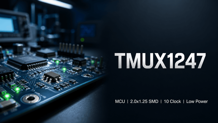
The TMUX1247 is a general-purpose, single-pole double-throw (SPDT) analog switch fabricated in CMOS technology. Designed by Texas Instruments (identified by "SCDS399" and "ti.com" references), this component is engineered to bidirectionally switch analog or digital signals. It targets applications requiring precision signal routing, low power consumption, and compact footprints, such as portable electronics, industrial automation, and communication interfaces. The device ensures Fail-Safe Logic operation, allowing control signals to be present before the supply voltage, preventing potential system latch-ups or damage during power-up sequences.
🎯 Typical Applications & Design Context
The TMUX1247 is ideally suited for space-constrained and power-sensitive designs.
- Communication Interfaces: 🔹 Multiplexing I2C or SPI buses to expand channel count without adding logic complexity.
- Industrial & Consumer: 🔹 Used in barcode scanners, motor drives, and building automation for sensor selection.
- RF/Antenna Systems: 🔹 Routing signals in active antenna systems (mMIMO AAS) or remote radio units.
- Operational Edge: Its wide supply range (1.08 V to 5.5 V) allows direct interfacing with both modern 1.8V logic and legacy 3.3V/5V systems, eliminating the need for level shifters in mixed-voltage designs.
📊 Key Technical Specifications
| Parameter | Condition | Spec/Value | Engineering Impact |
|---|---|---|---|
| Supply Voltage Range | Operating | 1.08 V to 5.5 V | ✅ High Flexibility: Supports battery-operated (1.2V) and industrial (5V) rails. |
| On-Resistance (RON) | VDD = 5V | 3 Ω (Max) | 💡 Low Loss: Minimizes voltage drop and signal distortion for analog precision. |
| Supply Current | Operating | 4 nA | 🔋 Ultra-Low Power: Essential for battery-powered devices; negligible quiescent current draw. |
| Logic Threshold | VDD > 1.8V | 1.8V Compatible | 🔒 Interface Safety: Ensures reliable switching driven by low-voltage MCUs/FPGAs. |
| Switching Time | Transition | 14 ns | 🚀 High Speed: suitable for high-frequency signal multiplexing and data acquisition. |
⚠️ Absolute Maximum Ratings & Process Limits
| Rating | Maximum Value | Critical Failure Risk (E-E-A-T Insight) |
|---|---|---|
| Supply Voltage (VDD) | -0.5 V to 6 V | 🛑 Exceeding 6V causes catastrophic oxide breakdown (CMOS destruction). |
| Input Current (ISEL) | ±30 mA | 🛑 Exceeding this current (e.g., from a voltage spike or miswired driver) fuses the bond wire or damages the ESD clamp diode, leading to permanent open circuits. |
| Continuous Current (Sx, D) | ±50 mA | 🚨 Thermal Runaway: While typical usage is low current, forcing >50mA (e.g., shorting a power rail through the switch) exceeds the package's power dissipation limit (PD), melting the SC70 package or causing signal drift. |
| Junction Temperature (TJ) | 150 °C | 🔥 Operating near this limit degrades the CMOS lifetime; ensure proper PCB copper dissipation for the 3Ω RON power. |
🧩 Package, Dimensions & Assembly Notes
- Package Type: SC-70 (SOT-353), 6-Pin.
- Dimensions: 2.00 mm × 1.25 mm (Nominal).
- Assembly Considerations: The tiny footprint (2.0x1.25mm) is highly sensitive to solder paste volume variations.
- Stencil Design: Ensure aperture reduction for the GND and VDD pads to prevent tombstoning or bridging, especially given the 0.65mm pitch.
- Thermal Management: Unlike power switches, this device dissipates minimal heat (RON * I2), but standard thermal relief pads are recommended for manual prototyping to avoid pad lifting during rework.
🔍 Procurement & Sourcing Insights
- Supply Chain Stability: As a TI device, availability is generally stable, but allocation periods can affect lead times.
- Alternative Validation: When sourcing from Huaqiangbei or non-authorized distributors, verify the On-Resistance (RON) and Leakage Current. Generic analog switches often have higher leakage (nA vs µA) which can corrupt high-impedance sensor readings.
- Counterfeit Risk: SC-70 packages are frequently re-marked. Verify the laser marking dating code consistency. Samples should be validated for the Fail-Safe Logic feature—if the chip heats up when VDD is 0V and SEL is high, it is a defective clone lacking proper ESD/rail protection structure.
- LDeepAI Action: We recommend securing a small verification batch to test logic thresholds before scaling to mass production.
❓ FAQ
Q: Can the TMUX1247 handle high-frequency SPI signals (e.g., 10 MHz)?
A: Yes. With a transition time of 14 ns and bandwidth suitable for general-purpose switching, it can handle typical SPI speeds (often <10 MHz in industrial contexts). However, for very high-speed SPI (>20 MHz), pay attention to the capacitance parameters; ensure the trace impedance is matched to prevent ringing, as the 3Ω RON is minor compared to trace impedance.
Q: What is the difference between this and a standard 74LVC1G3157?
A: The key differentiator is the wide supply range (down to 1.08V) and ultra-low power (4 nA). The TMUX1247 is optimized for battery-powered applications where the 74LVC1G3157 might have higher quiescent current or fail to operate reliably at 1.2V. Additionally, the TMUX1247's Fail-Safe logic offers better protection during power sequencing.
Q: Is it safe to apply 5V signals when the device is powered at 3.3V?
A: No. The Absolute Maximum Ratings state that signal voltage (Sx, D) must not exceed VDD + 0.5V. Applying 5V signals with a 3.3V supply can forward-bias the ESD protection diodes, causing uncontrolled current flow and potential device failure. Ensure signal levels are within the VDD range.
Q: How critical is the 0.1µF decoupling capacitor placement?
A: It is critical. Although the supply current is only 4 nA, the transition switching requires instantaneous charge. Place the capacitor as close as possible to the VDD and GND pins to stabilize the supply during fast switching (14 ns), preventing logic glitches on the SEL pin.