📌 Product Overview
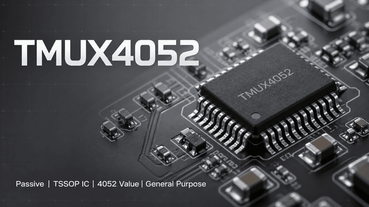
The TMUX4052 is a general-purpose complementary metal-oxide semiconductor (CMOS) multiplexer (MUX) configured as a dual 4:1 (1-of-4) channel switch. As part of Texas Instruments' TMUX405x series, it is designed to replace legacy industry-standard 4052 MUXes with significantly improved performance parameters.
Target Core Applications: This component is specifically engineered for high-voltage signal routing in industrial automation, battery test equipment, and heavy appliance boards. Its primary value proposition lies in its ability to handle wide supply voltages (up to 24V single rail or ±12V dual rail) while maintaining compatibility with modern low-voltage logic (1.8V), making it ideal for bridging legacy high-voltage analog front-ends with modern MCUs.
🎯 Typical Applications & Design Context
Based on its 24V rating and robust environmental specs, the TMUX4052 is best suited for:
- Industrial PLC & Control Modules: Routing analog sensor signals in harsh environments where voltage rails exceed standard 3.3V/5V logic limits.
- Battery Formation & Test Equipment: 🚀 The 24V support allows direct connection to high-cell-count battery packs without intermediate level shifters.
- Medical & Building Automation: 💡 Used in patient monitoring circuits or HVAC control systems where signal integrity and wide operating temperature ranges (-55°C to +125°C) are critical for regulatory compliance.
📊 Key Technical Specifications
| Parameter | Specification | Design Implication |
|---|---|---|
| Supply Range (Single) | 5V to 24V | Direct operation from industrial 24V bus; eliminates need for a 5V LDO. |
| Supply Range (Dual) | Up to ±12V | Supports bipolar analog signals (e.g., audio or sensor AC coupling). |
| Logic Interface | 1.8V Compatible | 📈 Driven directly by low-voltage MCUs/FPGAs even when VDD is 24V (Level shifting built-in). |
| Bandwidth | High | Low Capacitance (3pF) ensures minimal signal loading for data acquisition. |
| On-Resistance (Ron) | Low | Minimal voltage drop at full scale; reduces thermal self-heating. |
⚠️ Absolute Maximum Ratings & Process Limits
For mass production reliability, strictly observe the following boundaries to avoid permanent device damage:
| Rating | Limit | E-E-A-T Failure Analysis |
|---|---|---|
| VDD to VSS | -0.5V to 26V | 🔒 Exceeding 26V typically causes gate oxide breakdown, leading to catastrophic shorts between supply pins. |
| Analog Signal Current | ±10mA (Continuous) | Current flow >10mA through the switch can cause metal migration or latch-up, disconnecting the signal path permanently. |
| Operating Temp | -55°C to +125°C | While rated for high temp, derating is required near 125°C to avoid accelerated aging. |
| ESD (HBM) | 2000V | Standard handling is required; however, automated handling equipment (pick-and-place) must be grounded to prevent latent defects. |
🧩 Package, Dimensions & Assembly Notes
The TMUX4052 is typically available in the DYY (SOT-23-THIN, 16-pin) package.
- Assembly Challenge: 📉 The "Thin" SOT-23 variant has a lower thermal mass than standard TSSOP. During SMT reflow, the thermal profile must be carefully controlled to prevent tombstoning due to uneven heating of the ground vs. signal pads.
- PCB Layout: The 16-pin pitch is standard, but the pinout differs from older 4052 clones (typically CD4052). Engineers must verify the pin configuration—specifically the logic control pins (A0, A1, EN)—before printing, as this is a common source of NFF (No Fault Found) failures in prototypes.
🔍 Procurement & Sourcing Insights
The TMUX4052 is a current TI production part (Active status), but supply risks persist.
- Availability & Lead Times: TI distribution channels usually maintain stock, but allocation periods for industrial-grade parts can extend lead times to 20+ weeks during chip shortages.
- Alternative Risk: ⚠️ While advertised as "pin-compatible" with standard 4052s, many generic clones fail to support the 1.8V logic threshold while running at 24V. Swapping a TMUX4052 for a generic clone often results in logic failures (the switch won't turn on) if the clone lacks the TTL-logic translation.
- Sourcing Strategy: LDeepAI recommends verifying date codes strictly. Older stock or grey market units often suffer from leakage issues (Ioff) which drain batteries in test equipment.
❓ FAQ
Q: Can I use the TMUX4052 to replace a standard CD4052 in a legacy 12V system?
A: Yes. The TMUX4052 is designed as a drop-in performance upgrade. It is pin-to-pin compatible with the standard 4052 footprint but offers much lower Ron and charge injection, improving signal fidelity.
Q: Does the "1.8V logic compatible" feature mean I must power the chip at 1.8V?
A: No. A key advantage is its voltage translation capability. You can power the TMUX4052 at 24V (VDD) to switch high-voltage signals, while controlling the switch logic pins using a 1.8V or 3.3V MCU. This eliminates the need for external level shifters.
Q: What is the main difference between the TMUX4052 and the TMUX4053?
A: The TMUX4052 is a dual 4:1 Mux (two independent 4-to-1 switches), whereas the TMUX4053 is a triple 2:1 switch (three independent SPDT switches). They serve different routing topologies.
Q: Is the SOT-23-THIN package compatible with standard solder paste stencil designs?
A: Generally, yes. However, due to the "Thin" profile, aperture reduction for the thermal pad (if present) or ground terminals is recommended to prevent solder wicking and tombstoning during reflow.