📌 Product Overview
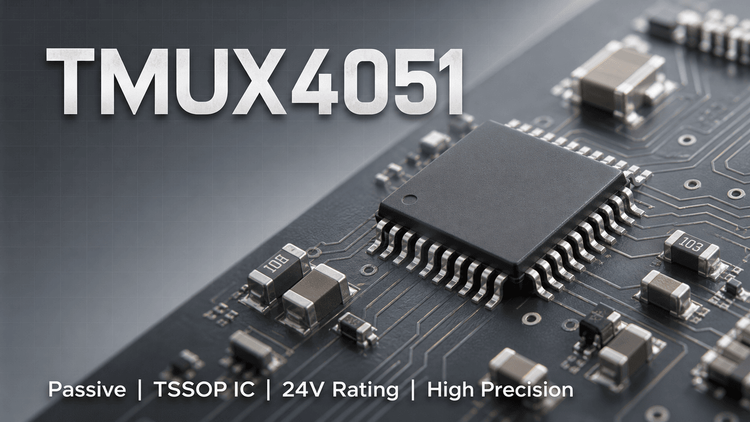
The TMUX4051 from Texas Instruments is a precision, 8:1 single-channel analog multiplexer designed to bridge high-voltage industrial signals with modern low-voltage logic. Unlike standard legacy 4051 devices, the TMUX4051 supports a wide supply range (up to 24V single or ±12V dual) while maintaining compatibility with 1.8V logic controllers. For engineering teams, this component serves as a critical signal routing interface in mixed-voltage environments, eliminating the need for level-shifters in many factory automation and test equipment designs. The primary selection variables here are the wide supply range (±12V), break-before-make switching to prevent signal contention, and extended industrial temperature range (-55°C to +125°C) for harsh environments.
🎯 Typical Applications & Design Context
- 🏭 Industrial Automation & Control: Designed for sensing PLCs and servo control loops where 24V sensor signals must be routed to low-voltage ADCs.
- 🔋 Battery Test Equipment: The high voltage rating (up to 24V) allows direct switching of high-cell-count battery strings without intermediate voltage dividers.
- 🏥 Medical Instruments: Suitable for medical-grade diagnostic equipment requiring robust signal isolation and wide voltage compliance (IEC 60601 considerations).
- ⚡ Power Delivery Systems: Used in UPS and BMS designs for bidirectional signal switching, leveraging the rail-to-rail operation capability.
📊 Key Technical Specifications
| Parameter | Value/Condition | Engineering Impact |
|---|---|---|
| Supply Voltage Range | Single: 5V to 24V Dual: ±12V | Supports legacy 24V industrial buses directly. |
| Logic Compatibility | 1.8V Logic Compatible | Enables direct interfacing with modern FPGAs/MCUs without level translators. |
| On-Resistance (Ron) | Typically low flat resistance | 💡 Minimizes signal distortion and voltage droop in precision paths. |
| Bandwidth | High Bandwidth (per datasheet curves) | Suitable for passing fast-edged control signals without significant attenuation. |
| Charge Injection | Low Charge Injection | Prevents output glitches (transients) when switching channels, crucial for precision measurement front-ends. |
| Switching Configuration | Break-Before-Make (BBM) | Prevents momentary short circuits between input channels during transition. |
| ESD Protection | 2000V HBM | 👇 Provides robust handling protection during assembly and field operation. |
⚠️ Absolute Maximum Ratings & Process Limits
| Parameter | Rating | Process Risk & E-E-A-T Insight |
|---|---|---|
| Supply Voltage (V+ to GND) | 26V | Risk: Exceeding this, even transiently (e.g., inductive kickback), can cause immediate oxide breakdown of the CMOS switches. |
| Analog Input Voltage | -0.5V to V++0.5V | Risk: ⚠️ Critical SMT Validation: If the analog input exceeds the supply rail (V+) by >0.5V, the internal ESD structures may forward bias, causing latch-up or signal leakage. Verify ground potential differences during power sequencing. |
| Continuous Current | Per Pin Limits | Risk: Overloading pins leads to localized heating and metal migration, causing open circuits over time. |
| Operating Temp (Junction) | -55°C to +125°C | Risk: While rated high, derating is required for self-heating. High Ron at elevated temps may affect signal accuracy. |
| Storage Temp | -65°C to +150°C | Risk: Exposure to extreme moisture during storage can compromise MSL (Moisture Sensitivity Level) performance. |
🧩 Package, Dimensions & Assembly Notes
- Available Packages:
- PW (TSSOP-16): Standard surface-mount, easy visual inspection.
- DYY (SOT-23-THIN-16): Ultra-compact solution for space-constrained portables.
- BQB (WQFN-16): Smallest footprint with exposed thermal pad for better heat dissipation.
- 🧠 SMT Validation Note: The WQFN (BQB) package requires careful X-ray inspection during SMT validation due to the hidden thermal pad solder joints. Ensure the PCB land pattern matches TI's latest reference design to avoid solder joint cracking under thermal cycling (-55°C cycles).
- Pin Compatibility: While pin-compatible with standard "4051" muxes, the VSS pin functionality supports negative voltages. Ensure the board layout separates high-voltage analog traces from sensitive 1.8V logic pins to prevent crosstalk.
🔍 Procurement & Sourcing Insights
- Supply Chain Reality: TMUX4051 is a mainstream TI component but is frequently impacted by lead time fluctuations in the +/-12V high-voltage MUX category.
- Alternative Validation: ⚠️ Risk Alert: While "Industry Standard 4051" devices exist, most competitors (e.g., ON Semi, Vishay) use legacy processes requiring >5V Vcc. The TMUX4051's unique 1.8V Logic feature makes it NOT a drop-in replacement for standard 5V-only logic 4051s if your system uses 1.8V GPIOs. Verify the Logic High (Vih) threshold carefully when validating alternatives.
- Traceability: As a high-reliability component, ensure reels are sourced from authorized channels to avoid "re-marked" pull-down parts that fail -55°C cold start testing.
❓ FAQ
Q: Can I replace a standard CD4051B with the TMUX4051 directly?
A: Yes, with caution. While the pinout is compatible, the TMUX4051 operates at much higher speeds and lower Ron. However, ensure your logic control pins can drive the required logic levels; the TMUX4051 is optimized for 1.8V logic but handles higher Vcc, whereas older 4000B series might have different input impedance characteristics.
Q: What is the most common failure mode in mass production for this device?
A: Signal contention. If the system software enables multiple inputs simultaneously before the switch fully settles (ignoring the Break-Before-Make delay), it can cause shorted inputs. Additionally, exceeding the analog input voltage rating relative to the supply rail (Vdd) is a common failure during power-up sequencing.
Q: Why would I choose the TMUX4051 over a cheaper generic MUX?
A: 3pF Capacitance and ±12V Support. Generic MUXs often restrict signal swing to the positive rail. If your application involves AC signals swinging below ground (e.g., audio or bipolar sensors), the TMUX4051's dual-supply capability and low charge injection are essential for signal integrity.
Q: Does the 1.8V logic support work if VDD is only 3.3V?
A: Yes. The datasheet specifies that the logic inputs are 1.8V compatible across the full supply range (5V to 24V). This allows a low-voltage MCU to control a high-voltage analog path (24V) without any level shifters.