📌 Product Overview
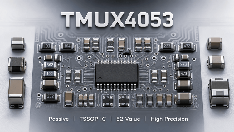
The TMUX4053 from Texas Instruments is a precision 2:1, 3-channel complementary metal-oxide semiconductor (CMOS) multiplexer (MUX). It is designed to handle wide voltage ranges (±12V dual supply or single 24V) while offering logic compatibility with modern 1.8V controllers. 💡 This component serves as a critical interface bridge in industrial automation, battery test equipment, and power delivery systems, enabling high-voltage signal routing controlled by low-voltage logic. For design engineers, the selection variable here is robustness: the ability to switch high-voltage analog signals without back-powering the logic supply or suffering from leakage currents.
🎯 Typical Applications & Design Context
The TMUX4053 is ideally suited for applications requiring high-voltage signal switching and rail-to-rail operation.
- Industrial Automation & Control: Used for sensor multiplexing in PLCs where 24V industrial field signals must be routed to low-voltage ADCs.
- Battery Formation & Test Equipment: Essential for managing high-cell-count battery stacks where the channel voltage range exceeds standard 5V or 12V MUX capabilities.
- Power Delivery & Protection Systems: Enables path switching for monitoring high-voltage rails (up to 24V) without requiring external level shifters.
- Why it fits: The device supports asymmetric supplies (e.g., VDD = 12V, VSS = –5V), allowing it to handle bipolar signals often found in biomedical or specialized instrumentation, bridging the gap between legacy high-voltage analog front-ends and modern digital logic.
📊 Key Technical Specifications
| Parameter | Value/Condition | Significance |
|---|---|---|
| Supply Voltage Range | Single: 5V to 24V Dual: ±12V | Covers legacy and industrial voltages; robust against supply surges. |
| Logic Compatibility | 1.8V Logic Input | Direct drive from modern FPGAs/MCUs without level translators. |
| On-Resistance ($R_{on}$) | Typically low (Check Datasheet Curve) | Low $R_{on}$ ensures signal integrity for precision analog measurements. |
| Bandwidth | High Speed (Check $t_{transition}$) | Suitable for passing fast-edged control signals or PWM waveforms. |
| Charge Injection | Low | Minimizes voltage glitches during switching, critical for accurate sampling. |
| Operating Temperature | –55°C to +125°C | Qualified for harsh industrial and extended automotive environments. |
⚠️ Absolute Maximum Ratings & Process Limits
Exceeding these ratings risks immediate silicon damage or latent reliability failures.
| Parameter | Rating | Failure Mode / Process Risk |
|---|---|---|
| Supply Voltage ($V_{DD}$ to GND) | 26V | Exceeding 26V causes oxide breakdown, permanently shorting VDD to GND. |
| Analog Signal Current | ±20 mA (Continuous) | Overcurrent leads to metal migration and eventual open circuit failure. |
| ESD Protection (HBM) | 2000 V | Handling without proper grounding can gate-oxide damage (latent defects). |
| Operating Temp | –55°C to +125°C | Operating near or beyond $T_{max}$ accelerates aging and parameter drift. |
🚨 E-E-A-T Insight: Pay close attention to the Break-Before-Make (BBM) timing. While BBM prevents momentary shorting of input channels, the transition time ($t_{transition}$) is the critical window. If the load is highly capacitive, the voltage rate of change ($dV/dt$) during this open-circuit phase can induce ringing. Ensure the downstream sampling ADC avoids this transition window to prevent "glitch" capture in production firmware.
🧩 Package, Dimensions & Assembly Notes
The TMUX4053 is available in the BQB (WQFN, 16-pin) package (as well as TSSOP and SOT-23 variants for the 4051/52 family).
- WQFN (16-pin): Features a thermal pad on the bottom. 👇 This is critical for heat dissipation.
- SMT Validation: The thermal pad requires solder paste definition (Aperture) in the stencil design. Insufficient paste coverage on the thermal pad will cause tombstoning or thermal lift during reflow.
- Land Pattern: Do not use the footprint for the older CD4053 or 74HC4053 blindly. Pin 1 locations and thermal pad dimensions differ. Verify the "Mechanical, Packaging, and Orderable Information" section before generating Gerber files.
🔍 Procurement & Sourcing Insights
From a supply chain perspective, the TMUX4053 offers high reliability but requires careful lifecycle management.
- Lifecycle Status: TI analog switches are generally in "Active Production," but allocate for lead times of 12-20 weeks for specific package variants (like TSSOP) during industry shortages.
- Alternative Risk: ⚠️ Beware of Direct Substitutes. Competitor "drop-in" MUXes (e.g., from Maxim or ADI) may have different Logic Input thresholds ($V_{IH}$/$V_{IL}$). A substitute claiming 1.8V logic might fail if the $V_{DD}$ is at 5V and the threshold curves differ. Always re-validate the Logic High/Low voltage specs at your specific operating voltage.
- Authenticity: Sourced TI components from non-authorized channels must be inspected for "Black Top" marking anomalies. LDeepAI supports X-Ray verification for die consistency to mitigate Huaqiangbei scrap risks.
❓ FAQ
Q: Can I replace my legacy CD4053 with the TMUX4053 without changing my PCB?
A: No. While the TMUX405x family is pin compatible with industry-standard 4053 muxes in terms of signal pins, the physical footprint often differs (e.g., WQFN vs DIP/SOIC). If using the TSSOP version, pin mapping is compatible, but you must verify the supply voltage and logic input levels, as the TMUX4053 has stricter logic requirements than a bipolar-based 4053.
Q: The datasheet mentions 1.8V logic. Does this work if my analog supply ($V_{DD}$) is 24V?
A: Yes. This is the key feature of the TMUX4053. The Logic supply pins ($V_{DD}$) typically power the switch, but the logic inputs (SEL, EN) are referenced to translate 1.8V levels even when the switch is passing 24V signals. Verify the $V_{Logic}$ threshold charts in the datasheet to ensure noise immunity.
Q: Why is my signal distorted when switching high-frequency loads?
A: Check the On-Resistance Flatness ($R_{on}$ flatness over $V_{signal}$). If the $R_{on}$ varies significantly as the input signal approaches the rails, it introduces distortion. Also, verify the Charge Injection spec; high-speed switching of high-impedance nodes can cause voltage steps due to injected charge.
Q: Are there SMT process concerns for the WQFN package?
A: The Thermal Pad is the primary concern. It must be soldered to the ground plane for electrical and thermal reasons. In mass production, use X-Ray inspection to verify voiding is under 15% inside the thermal pad; otherwise, thermal performance will degrade, leading to potential failure in high-temperature environments.