📌 Product Overview
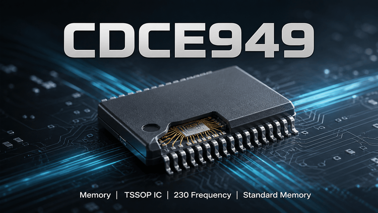
The CDCE949 is a high-performance, 4-PLL programmable clock synthesizer designed to replace fixed oscillators and crystal multipliers in complex systems. Unlike standard clock generators, it integrates flexible LVCMOS output drivers and on-chip EEPROM, making it ideal for generating up to 9 independent clock frequencies (up to 230MHz) from a single input reference. 💡 It is specifically engineered for systems requiring precise frequency multiplication and Spread Spectrum Clocking (SSC) for EMI reduction, such as set-top boxes, DTVs, and networking infrastructure. Engineers select this component to solve clock tree complexity while maintaining 60ps (typical) period jitter performance.
🎯 Typical Applications & Design Context
The CDCE949 excels in high-density consumer electronics and industrial networking where board space and EMI control are critical. 👇 Typical use cases include:
- D-TV & STBs: Synchronizing video decoders, audio DACs, and backplanes from a single 27MHz crystal, reducing component count.
- Networking (Ethernet/WLAN/GPS): Generating PHY clocks and multi-rate frequencies for FPGAs without needing multiple oscillators.
- Computing: Replacing multiple crystals in TI-DaVinci™ or OMAP™ based designs, ensuring 0ppm frequency accuracy across the system.
- Why it fits: The ability to program Spread Spectrum Clocking (SSC) via internal register settings allows designers to pass stringent EMI compliance tests without adding costly filtering components.
📊 Key Technical Specifications
💡 Decision-critical parameters derived from rated conditions (3.3V, 25°C)
| Parameter | Value/Condition | Design Impact |
|---|---|---|
| Output Frequency Range | Up to 230 MHz | Covers high-speed interfaces (USB, Ethernet) and moderate-speed logic. |
| Input Frequency (Crystal) | 8 MHz to 32 MHz | Determines the fundamental reference stability; ensures common crystal availability. |
| Period Jitter (Typical) | 60 ps | Critical margin for high-speed PHY (e.g., Gigabit Ethernet) Bit Error Rate (BER). |
| Output Supply (VDDOUT) | 3.3V or 2.5V (CDCE949) | Must match the I/O voltage of the downstream load (FPGA/ASIC). |
| Core Supply (VDD) | 1.8 V | Requires a stable LDO rail separate from I/O voltage. |
| Operating Temp | –40°C to 85°C | Standard commercial range; derating required for high-ambient industrial enclosures. |
⚠️ Absolute Maximum Ratings & Process Limits
🚨 Exceeding these limits risks permanent silicon damage or catastrophic system failure.
| Parameter | Rating | E-E-A-T Insight: Failure Consequence |
|---|---|---|
| Supply Voltage (VDD, VDDOUT) | –0.5V to 4.6V | Risk: Oxide breakdown. Over-voltage (e.g., 5V mis-wire) destroys the internal PLL circuitry instantly. |
| Input Current (CLK_in) | –50mA to 50mA | Risk: ESD latch-up. Signal rings or reflections exceeding this clamp current can trigger thermal runaway. |
| Total Power Dissipation | See Thermal Data | Risk: Sustained high-frequency output on all 9 channels raises junction temp ($T_J$), potentially causing PLL unlock or thermal shutdown. |
| Storage Temperature | –65°C to 150°C | Risk: Moisture ingress. Pre-conditioning (baking) is mandatory if MSL > 3 to avoid "popcorning" during reflow. |
🧩 Package, Dimensions & Assembly Notes
The CDCE949 is housed in a TSSOP-24 (Package Code: PW) with a nominal footprint of 7.8mm × 6.4mm. 👇
- SMT Validation: The TSSOP-24 has a 0.65mm pitch. Ensure stencil apertures are optimized for gull-wing leads to prevent solder bridging.
- Thermal Pad: Note that while this is a leaded package, the primary thermal path is through the leads to the ground planes. Ensure adequate thermal vias under the GND pins.
- Layout Sensitivity: Being a clock generator, the Xin/CLK_in trace is highly sensitive. Keep it short, shielded, and away from switching power supplies (like DC-DC converters) to avoid phase noise degradation.
🔍 Procurement & Sourcing Insights
- Supply Chain Risk: The CDCE949 is a mature TI component. However, specific speed grades or the 1.8V variant (CDCEL949) may have longer lead times.
- Fake & Gray Market: ⚠️ In high-mix markets, watch out for "re-marked" TSSOP packages. Verify package laser marking contrast; counterfeits often have softer, blurry laser etching.
- Alternative Sourcing: Direct pin-to-pin replacements are rare. Most alternatives (e.g., IDT or Renesas) require PCB layout changes due to different pin mappings.
- Inventory Strategy: LDeepAI recommends securing the Programming Kit (TI Pro-Clock™) early. Reprogramming generic stock to custom frequencies is faster than waiting for factory-locked orders.
❓ FAQ
Q: Can I use the CDCE949 to replace a standard fixed crystal oscillator (XO)?
A: Yes, this is a primary use case. By configuring one of the 9 outputs (e.g., Y1) to your desired frequency (e.g., 24MHz) and using the other 8 outputs for other system clocks, you effectively replace the XO and additional clock buffer chips. However, ensure your layout keeps the loop filter area quiet.
Q: What is the difference between CDCE949 and CDCEL949?
A: The main difference is the Output Supply Voltage (VDDOUT). The CDCE949 supports 2.5V or 3.3V outputs (standard LVCMOS), while the CDCEL949 is optimized for 1.8V outputs. Using the wrong variant will result in level mismatch (voltage incompatibility) with your load device, damaging the FPGA or ASIC inputs.
Q: How do I handle the SSC (Spread Spectrum) setup for production?
A: SSC settings are stored in the internal EEPROM. You must program the modulation depth and center/down spread profiles via I2C (SDA/SCL) before final assembly or utilize a generic configuration that is programmed in-system (ISP) during the board's initialization sequence. Ensure the control pins (S0/S1/S2) are not left floating to avoid random frequency switching.
Q: What is the risk if the input crystal frequency deviates?
A: The PLL multiplies the input error. Even a ±50ppm crystal error will be multiplied by the N-divider. For Ethernet applications, this can push the clock out of the specified ±50ppm tolerance window, causing link drops. Use a "Fundamental Mode" crystal with tight ±20ppm or better tolerance.