📌 Product Overview
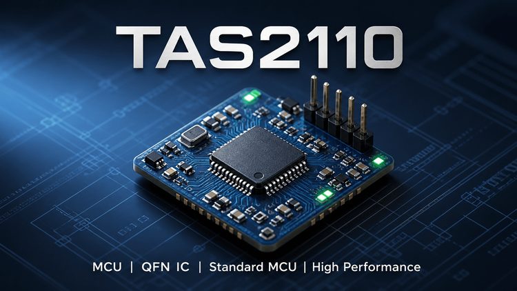
The TAS2110 is a high-efficiency, digital input Class-D audio amplifier featuring an algorithmically controlled 11-V Class-H boost converter. Designed to maximize battery life in portable smart devices, it utilizes a Look-Ahead Algorithm to dynamically adjust the boost voltage, minimizing power loss compared to fixed boost architectures. 💡
Ideally suited for Smart Speakers, Bluetooth Audio, and IoT devices, this device integrates power management and high-quality audio output into a single 4.5mm x 4mm QFN package. For system designers, the critical decision variables shift from simple power ratings to GUI-based algorithm tuning and PCB layout thermal reliability under peak drive conditions.
🎯 Typical Applications & Design Context
The TAS2110 excels in battery-operated audio systems requiring high output power without draining the battery.
- Smart Speakers with Voice Assistance: The device supports I2S/TDM inputs up to 96 KSPS, making it compatible with modern voice processing DSPs. Its low quiescent current (<1 µA in shutdown) ensures "always-listening" features do not compromise battery standby time.
- Portable & Wireless Speakers: The integrated Class-H boost allows 6.1 W peak output into 4 Ω even from a low 3.6 V battery voltage, enabling "loud" audio performance in compact form factors where thermal headroom is limited.
- Smart Home & IP Cameras: Integrated VBAT tracking and Advanced Brownout Protection prevent system crashes during high-bass peaks, a critical requirement for hardwired or low-power wireless devices.
📊 Key Technical Specifications
| Parameter | Specification | Test Condition |
|---|---|---|
| Output Power | 6.1 W (Peak) | 1% THD+N, VBAT = 3.6 V, 4 Ω Load |
| Efficiency | 83.5% | 1 W Output, 8 Ω Load |
| Supply Voltage (VBAT) | 2.7 V to 5.5 V | Battery Input Range |
| Logic Voltage (VDD) | 1.65 V to 1.95 V | Digital Core Supply |
| Shutdown Current | < 1 µA | Hardware Shutdown Mode |
| Audio Interface | I2S / TDM (8 ch, 32-bit) | Sample Rates: 7.35 KSPS to 192 KSPS |
| Control Interface | I2C | 4 Selectable Addresses |
💡 Note: While peak power is 6.1 W, continuous power capability is strictly limited by the PCB thermal design. The "Typical Characteristics" in the full datasheet must be cross-referenced with your specific PCB stack-up.
⚠️ Absolute Maximum Ratings & Process Limits
Exceeding these ratings permanently damages the device. High failure risk areas in mass production include reverse polarity and voltage spikes.
| Parameter | Rating | Unit |
|---|---|---|
| VBAT (Supply Input) | -0.3 to 5.8 | V |
| PVDD (Boost Output) | -0.3 to 13 | V |
| Total Power Dissipation | Limited by TJMAX (150°C) | mW |
| Junction Temp (TJ) | -40 to 150 | °C |
| ESD Rating (HBM) | 2000 | V |
🚨 E-E-A-T Insight:
- Brownout & Clipping: If VBAT tracking parameters are incorrectly configured via the GUI, the amplifier may attempt to draw excessive current from a depleted battery. While the IC has internal protection, aggressive tuning without verifying battery IR (Internal Resistance) can lead to unexpected system resets (Brownout) during loud music transients.
- Boost Inductor Saturation: The integrated boost switches at high frequency. Using an inductor with insufficient saturation current rating will cause the inductor to overheat and potentially short the SW (Switch) pin to ground, destroying the IC.
🧩 Package, Dimensions & Assembly Notes
- Package Type: 32-Pin QFN (4.5 mm x 4.0 mm).
- Thermal Pad: The center pad (exposed die attach pad) is the primary thermal path. It must be soldered to the PCB ground plane.
- PCB Stack-up: The datasheet explicitly mentions 2-layer board design compatibility. However, for 6.1 W operation, a 2-layer board requires careful copper pour management under the device to avoid thermal throttling.
- SMT Reflow: Standard lead-free reflow profiles (peak temp ~260°C) apply. Ensure the thermal pad has sufficient via stitching to inner ground layers to dissipate heat during the reflow process to prevent tombstoning or poor pad wetting.
🔍 Procurement & Sourcing Insights
When sourcing the TAS2110 for mass production, consider the following supply chain risks and strategies:
- Lifecycle & Origin: As a specialized Audio IC (Manufacturer: Texas Instruments based on doc style), verify the "Production Data" status. Avoid "Recycled" or "Pull" stock from the open market; audio performance degrades significantly if the device has been subject to previous electrical stress or moisture ingress (MSL handling).
- Fake vs. Genuine: Counterfeit components in this class often have incorrect internal boost regulator doping, leading to failure under 4 Ω load. Always source from authorized franchises or verify traceability codes.
- Alternative Sourcing: Drop-in replacements are rare due to the specific Class-H Boost Algorithm. If availability is low, the entire GUI tuning configuration and inductor selection may need to be re-qualified for any alternative part.
❓ FAQ
Q: Can I replace the TAS2110 with a standard Class-D amplifier without the boost?
A: No. The TAS2110 generates its own internal 11V PVDD from the battery. A standard amp requires a higher external voltage. Replacing it without considering the boost inductor removal and PCB layout change will result in no sound output.
Q: What is the most common cause of failure during mass production?
A:PCB Thermal Issues. On 2-layer boards, insufficient copper area under the QFN pad causes the junction temperature to exceed 150°C during peak audio testing, triggering thermal shutdown. Ensure at least 1 sq. inch of copper pour connected to the ground pad.
Q: Is MCLK (Master Clock) strictly required?
A: The datasheet supports MCLK-free operation. This simplifies BOM cost and layout, as you do not need to route a high-frequency clock signal from the host processor, reducing EMI interference in smart speaker designs.
Q: How critical is the inductor selection?
A: Critical. The inductor must handle the peak switch current without saturating. Using a generic "standard" inductor often leads to audible buzzing (magnetic noise) or boost failure under heavy bass loads.