📌 Product Overview
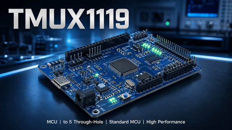
The TMUX1119 from Texas Instruments is a single 2:1 (SPDT) precision analog switch built on CMOS technology. It operates from a wide 1.08V to 5.5V supply, making it suitable for battery-powered and mixed-voltage systems. Its defining traits are 3pA leakage current, 1.8Ω on-resistance, and –6pC charge injection, positioning it as a signal-chain component rather than a digital logic gate. Engineers evaluating it should focus on leakage performance at temperature, break-before-make behavior, and footprint compatibility across its two package options.
🎯 Typical Applications & Design Context
The datasheet targets precision measurement and low-power systems:
- Medical devices — ultrasound scanners, patient monitoring, glucose monitors, where picoamp-level leakage preserves measurement accuracy
- Test & measurement — semiconductor test equipment and data acquisition systems, where low charge injection minimizes sample distortion
- Optical modules and remote radio units — low supply current (3nA) supports power-constrained designs
- Industrial controls — PLCs, analog input modules, flow transmitters, and battery test equipment
The bidirectional rail-to-rail signal path (GND to VDD) means one part can switch both analog sensor signals and digital logic lines, simplifying BOM consolidation.
📊 Key Technical Specifications
| Parameter | Value | Design Implication |
|---|---|---|
| Supply range (VDD) | 1.08V – 5.5V | Single rail across 1.2/1.8/3.3/5V systems |
| On-resistance (RON) | 1.8Ω | Low signal attenuation for low-impedance paths |
| Off/on leakage | 3pA | Critical for precision ADC front ends |
| Charge injection | –6pC | Reduced glitching in sample-and-hold circuits |
| Supply current | 3nA | Portable/battery applications |
| Logic threshold | 1.8V-compatible | Direct drive from MCU GPIO |
| Operating temperature | –40°C to +125°C | Industrial-grade coverage |
| Switching mode | Break-before-make | Prevents momentary source-to-source short |
| ESD (HBM) | 2000V | Standard handling class |
💡 Note: RON varies with supply voltage and signal level — verify the derating curve at your actual VDD, not just the 5V headline number.
⚠️ Absolute Maximum Ratings & Process Limits
| Limit | Rating |
|---|---|
| VDD supply voltage | –0.5V to 6V |
| SEL logic pin voltage | –0.5V to 6V |
| SEL pin current | ±30mA |
| Source/drain voltage | –0.5V to VDD + 0.5V |
| Continuous S/D current | Per datasheet curve (IDC ±10%) |
👇 Two practical failure points:
- S/D voltage must never exceed VDD + 0.5V. In mixed-voltage boards where the TMUX1119 supply rails up before the signal source, or during hot-plug events, source pins can be back-driven above the rail — causing latch-up or permanent leakage degradation. The fail-safe logic protects only the SEL pin, not the signal path.
- Fail-safe logic allows SEL before VDD, which simplifies power sequencing but is often misread as full input protection — it is not. Verify board-level sequencing during validation.
🧩 Package, Dimensions & Assembly Notes
Two pin-compatible-in-function packages are offered:
| Package | Size | Notes |
|---|---|---|
| DCK (SC70-6) | 2.0mm × 2.1mm | Smallest footprint; check land pattern for reflow opens |
| DBV (SOT-23-6) | 2.9mm × 2.8mm | Easier inspection and rework; preferred for prototypes |
The 6-pin layout (SEL, VDD, GND, S1, D, S2) is standard across the SC70/SOT-23 2:1 switch ecosystem, easing second-source qualification. TI recommends a 0.1µF–10µF decoupling capacitor at VDD. MSL and reflow limits follow standard JEDEC profiles for these package types; fine-pitch SMT lines should confirm SC70 solder-joint inspection criteria (X-ray or 45° AOI angle) in mass production.
🔍 Procurement & Sourcing Insights
- 💡 Lifecycle & supply: TI marks this as production data; standard TI lead times apply, but SC70-6 precision switches see allocation spikes during demand surges — secure buffer stock for 12-month programs.
- 🔒 Traceability: Huaqiangbei market stock of TI marking code DCK packages carries rebranding risk; require date-code and lot-level COC verification.
- ✅ Alternative validation: Pin-compatible alternatives exist (e.g., similar SPDT switches), but leakage specs differ significantly — 3pA class performance is not universal. Re-verify leakage at 85°C before cross-qualifying.
- 📈 Sample & MOQ: LDeepAI supports sample quantities for engineering validation and volume quoting with full traceability for TMUX1119 in both DCK and DBV options.
❓ FAQ
Q: Can I substitute TMUX1119 with a generic 4053-type analog switch?
A: Not directly for precision applications. CD4053-class parts have leakage in the nA range, orders of magnitude higher than 3pA. Only consider substitution for non-precision digital routing, after bench leakage verification.
Q: Is the SC70 (DCK) and SOT-23 (DBV) footprint interchangeable?
A: Functionally pin-compatible, but not footprint-identical. PCB layout must use the correct land pattern; a SC70 layout cannot accept SOT-23 without redesign.
Q: What happens if SEL is driven before VDD?
A: The fail-safe logic permits it safely — control pins tolerate up to 6V independent of supply. However, signal pins (S1/S2/D) are not protected this way.
Q: Why does my measured RON exceed 1.8Ω?
A: RON is specified at 5V supply with specific signal conditions. At 1.8V or 1.2V supply, RON rises substantially — consult the electrical characteristics tables for your VDD.
Q: How do I verify authentic TI parts?
A: Check date-code consistency, lot traceability against TI shipping documents, and order through traceable channels. LDeepAI provides lot-level verification support.