📌 Product Overview
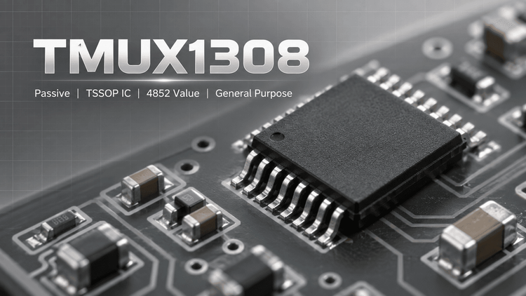
The TMUX1308 (8:1, 1-channel single-ended) and TMUX1309 (4:1, 2-channel differential) are TI's 5-V CMOS analog multiplexers with integrated injection current control. They route analog or digital signals bidirectionally from GND to VDD in test systems, data center switching, and remote radio units. The critical selection variables are supply range (1.62–5.5 V), on-resistance, off-leakage, and package footprint compatibility with legacy 4051/4851 designs.
🎯 Typical Applications & Design Context
- Diagnostics and monitoring — injection current control allows disabled channel inputs to exceed the supply rail, eliminating external diode/resistor protection networks. This simplifies BOM and frees PCB area.
- Data center switch, rack servers, RRU — low capacitance and rail-to-rail operation support signal-path integrity.
- Electricity meters, string inverters, IP cameras — wide supply range and fail-safe logic tolerate noisy or unstable power sequencing.
- Back-powering protection — no internal ESD diode to VDD prevents unintended powering of the supply rail, a common failure mode when replacing 4051 devices.
📊 Key Technical Specifications
| Parameter | TMUX1308 / TMUX1309 |
|---|---|
| Configuration | 8:1, 1-ch (TMUX1308) / 4:1, 2-ch (TMUX1309) |
| Supply voltage | 1.62 V to 5.5 V |
| Signal range | GND to VDD, rail-to-rail, bidirectional |
| Logic threshold | 1.8 V logic compatible (TTL/CMOS) |
| Switching behavior | Break-before-make |
| Supply sequencing | Fail-safe logic — control pins may lead VDD |
| Functional safety | Functional Safety-Capable, documentation available |
💡 On-resistance is specified with ΔR tested at VDD/2 — verify flatness across your actual signal swing, especially at 1.8 V and 2.5 V supplies where limits were revised in Rev. E of the datasheet.
⚠️ Absolute Maximum Ratings & Process Limits
| Limit | Practical Impact |
|---|---|
| Signal range beyond VDD permitted (on disabled paths) | Safe only via internal injection current control; do not assume standard CMOS mux rules |
| No ESD diode to VDD | Inputs won't clamp to supply — verify downstream ESD strategy at connector interfaces |
| Control-pin voltage before VDD (fail-safe) | Tolerates hot-plug sequencing, but sustained over-voltage still damages device |
| MSL rating (per package, TSSOP-16/SOT-23-Thin/WQFN-16) | WQFN-16 (BQB) requires tighter moisture control; floor-life violations cause popcorn cracking during reflow |
⚠️ E-E-A-T field note: The most common replacement failure when swapping from a 4051 occurs during SMT validation — teams reuse legacy reflow profiles for the SOT-23-THIN (DYY) package without adjusting ramp rates, causing wetting issues on the thin-lead outline. Additionally, designers assuming a standard VDD clamp diode mis-specify input protection, and the unintended absence of the diode path changes system ESD behavior at board-level testing.
🧩 Package, Dimensions & Assembly Notes
| Package | Body Size (NOM) | Notes |
|---|---|---|
| PW (TSSOP, 16) | 5.00 mm × 4.40 mm | Drop-in for legacy 4051 TSSOP footprints |
| DYY (SOT-23-THIN, 16) | 4.20 mm × 2.00 mm | Low-profile; verify land pattern and stencil aperture |
| BQB (WQFN, 16) | 3.50 mm × 2.50 mm | Requires center thermal pad paste control and X-ray inspection |
💡 TMUX1308 is pin-compatible with industry-standard 4051 and 4851 multiplexers; TMUX1309 matches 4051/4052, 4851/4852 footprints. Layout guidance in datasheet Section 12 recommends short, symmetric source/drain routing to minimize crosstalk and off-isolation degradation. For WQFN assembly, confirm paste printing on the exposed pad — voiding here degrades ground return, not thermal dissipation, since the device is low power.
🔍 Procurement & Sourcing Insights
- 🔒 Authenticity risk: TMUX13xx devices are frequently re-marked from industrial 4051 stock in Huaqiangbei channels. Verify date codes, laser marking depth, and request TI Certificate of Conformance (CoC) for production lots.
- 📈 Lead time: TI analog muxes typically run 8–16 weeks during allocation cycles; secure buffer stock once design is frozen.
- 🧪 Sample support: Samples available for engineering validation; production MOQ is typically reel-based (3,000 pcs for SOT-23-THIN, 2,500 pcs for TSSOP-16).
- 🔄 Alternative validation: While pin-compatible with 4051/4851, the injection current control feature changes over-voltage behavior — re-verify all input protection circuits before design release. Contact LDeepAI for cross-brand alternative cross-reference and validated second-source options.
❓ FAQ
Q: Can I directly replace CD4051/HC4051 with TMUX1308?
A: Electrically, yes — the TMUX1308 is pin-compatible. But the TMUX1308 lacks an internal ESD diode to VDD, which changes over-voltage clamping behavior. Re-validate your protection circuit.
Q: Is TMUX1308 safe if input signals exceed VDD?
A: Yes, on disabled channels — internal injection current control isolates them. This eliminates external diode/resistor networks used with standard 4051 devices.
Q: Which package should I choose for a low-profile design?
A: SOT-23-THIN (DYY) at 2.00 mm body height, or WQFN (BQB) at 3.50 mm × 2.50 mm for dense layouts. WQFN requires tighter SMT moisture control.
Q: Is the TMUX1309 pin-compatible with CD4052?
A: Yes — TMUX1309 matches the 4052/4852 footprint as a 4:1 differential mux. Confirm control pin logic compatibility before release.
Q: What supply sequencing is required?
A: Fail-safe logic allows control inputs to be applied before VDD. Hot-plug the control lines safely, but never sustain signal over-voltage on enabled paths.
Q: How do I verify TMUX1308 authenticity from third-party channels?
A: Request TI CoC, verify laser-mark depth and font under magnification, cross-check date code against TI lot records, and perform X-ray inspection for WQFN versions.